- 您現(xiàn)在的位置:買賣IC網(wǎng) > PDF目錄370900 > M38195E6-XXXFS (Mitsubishi Electric Corporation) SINGLE-CHIP 8-BIT CMOS MICROCOMPUTER PDF資料下載
參數(shù)資料
| 型號: | M38195E6-XXXFS |
| 廠商: | Mitsubishi Electric Corporation |
| 英文描述: | SINGLE-CHIP 8-BIT CMOS MICROCOMPUTER |
| 中文描述: | 單芯片8位CMOS微機 |
| 文件頁數(shù): | 43/60頁 |
| 文件大小: | 664K |
| 代理商: | M38195E6-XXXFS |
第1頁第2頁第3頁第4頁第5頁第6頁第7頁第8頁第9頁第10頁第11頁第12頁第13頁第14頁第15頁第16頁第17頁第18頁第19頁第20頁第21頁第22頁第23頁第24頁第25頁第26頁第27頁第28頁第29頁第30頁第31頁第32頁第33頁第34頁第35頁第36頁第37頁第38頁第39頁第40頁第41頁第42頁當(dāng)前第43頁第44頁第45頁第46頁第47頁第48頁第49頁第50頁第51頁第52頁第53頁第54頁第55頁第56頁第57頁第58頁第59頁第60頁
43
3819 Group
SINGLE-CHIP 8-BIT CMOS MICROCOMPUTER
MITSUBISHI MICROCOMPUTERS
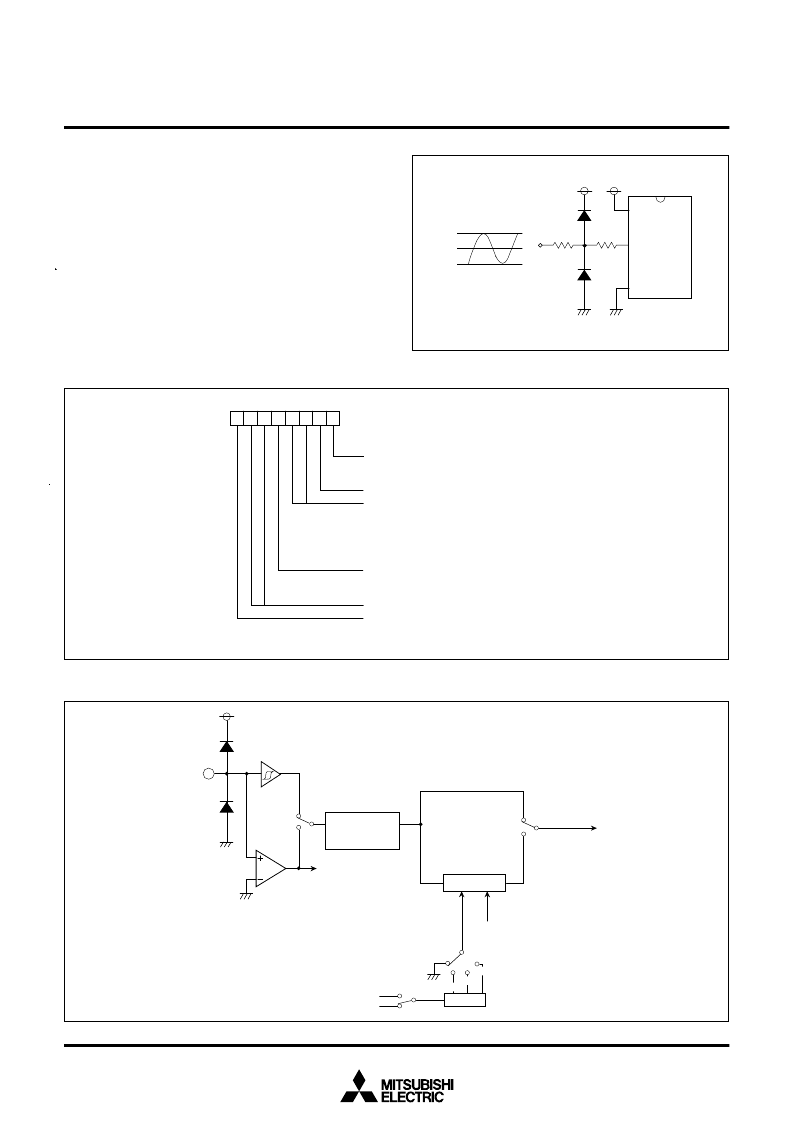
ZERO CROSS DETECTION CIRCUIT
The zero cross detection circuit compares the voltage applied to
P4
5
/INT
1
/ZCR pin and V
SS
. The result can be read from the zero
cross detection circuit input bit (bit 7) of the zero cross detection
control register. It is set to “1” when the input voltage is higher than
V
SS
and to “0” when it is lower than V
SS
. The input signal to P4
5
/
INT
1
/ZCR pin can select to either pass through the zero cross de-
tection comparator or not to do.
When using 100 V AC as input signal, insert an external circuit be-
tween it and P4
5
/INT
1
/ZCR pin. Set the input current limiting
resistors used in the external circuit to a value which satisfies the
absolute maximum rating of port P4
5
.
Fig. JE-1 External circuit example for zero cross detection
Fig. JE-3 Block diagram of zero cross detection circuit
Fig. JE-2 Structure of zero cross detection control register
V
CC
R
1
R
2
P4
5
/INT
1
/ZCR
V
SS
100V AC
Zero cross detection ON/OFF selection bit
0 : Without passing through zero cross detection comparator
1 : Passing through zero cross detection comparator
Not used (returns “0” when read)
Noise filter sampling clock selection bits (INT
1
)
b3 b2
0 0 : Not use noise filter
0 1 : f(X
IN
)/64 or f(X
CIN
)/64
1 0 : f(X
IN
)/128 or f(X
CIN
)/128
1 1 : f(X
IN
)/256 or f(X
CIN
)/256
One-sided/both-sided edge detection selection bit
0 : One-sided edge detection
1 : Both-sided edge detection
Not used (return “0” when read)
Zero cross detection circuit input bit (read only)
0 : Less than 0 V
1 : 0 V or more
b7
Zero cross detection control register
(ZCRCON : address 0039
16
)
b0
P4
5
/INT
1
/ZCR
Zero cross detection
ON/OFF selection bit
“0”
“1”
Zero cross detection
circuit input bit
Rising/falling
edge switch
Noise filter
When not using
the filter
When using
the filter
INT
1
/ZCR
interrupt request
One-sided/both-sided edge
detection selection bit
Noise filter sampling clock
selection bit
Zero cross detection comparator
f(X
CIN
)
f(X
IN
)
Divider
1/64
1/256
1/28
相關(guān)PDF資料 |
PDF描述 |
|---|---|
| M38195E8-XXXFP | SINGLE-CHIP 8-BIT CMOS MICROCOMPUTER |
| M38195E8-XXXFS | SINGLE-CHIP 8-BIT CMOS MICROCOMPUTER |
| M38195E9-XXXFS | SINGLE-CHIP 8-BIT CMOS MICROCOMPUTER |
| M38195EB-XXXFP | SINGLE-CHIP 8-BIT CMOS MICROCOMPUTER |
| M38195EB-XXXFS | SINGLE-CHIP 8-BIT CMOS MICROCOMPUTER |
相關(guān)代理商/技術(shù)參數(shù) |
參數(shù)描述 |
|---|---|
| M38197MA127F | 制造商:Panasonic Industrial Company 功能描述:IC |
| M38197MA131F | 制造商:Panasonic Industrial Company 功能描述:IC |
| M38197MA137F | 制造商:Panasonic Industrial Company 功能描述:IC |
| M38197MA161F | 制造商:Panasonic Industrial Company 功能描述:IC |
| M38197MA181F | 制造商:Panasonic Industrial Company 功能描述:IC |
發(fā)布緊急采購,3分鐘左右您將得到回復(fù)。