- 您現(xiàn)在的位置:買(mǎi)賣(mài)IC網(wǎng) > PDF目錄45037 > M37754S4CGP 16-BIT, 40 MHz, MICROCONTROLLER, PQFP100 PDF資料下載
參數(shù)資料
| 型號(hào): | M37754S4CGP |
| 元件分類(lèi): | 微控制器/微處理器 |
| 英文描述: | 16-BIT, 40 MHz, MICROCONTROLLER, PQFP100 |
| 封裝: | PLASTIC, QFP-100 |
| 文件頁(yè)數(shù): | 88/114頁(yè) |
| 文件大?。?/td> | 1116K |
| 代理商: | M37754S4CGP |
第1頁(yè)第2頁(yè)第3頁(yè)第4頁(yè)第5頁(yè)第6頁(yè)第7頁(yè)第8頁(yè)第9頁(yè)第10頁(yè)第11頁(yè)第12頁(yè)第13頁(yè)第14頁(yè)第15頁(yè)第16頁(yè)第17頁(yè)第18頁(yè)第19頁(yè)第20頁(yè)第21頁(yè)第22頁(yè)第23頁(yè)第24頁(yè)第25頁(yè)第26頁(yè)第27頁(yè)第28頁(yè)第29頁(yè)第30頁(yè)第31頁(yè)第32頁(yè)第33頁(yè)第34頁(yè)第35頁(yè)第36頁(yè)第37頁(yè)第38頁(yè)第39頁(yè)第40頁(yè)第41頁(yè)第42頁(yè)第43頁(yè)第44頁(yè)第45頁(yè)第46頁(yè)第47頁(yè)第48頁(yè)第49頁(yè)第50頁(yè)第51頁(yè)第52頁(yè)第53頁(yè)第54頁(yè)第55頁(yè)第56頁(yè)第57頁(yè)第58頁(yè)第59頁(yè)第60頁(yè)第61頁(yè)第62頁(yè)第63頁(yè)第64頁(yè)第65頁(yè)第66頁(yè)第67頁(yè)第68頁(yè)第69頁(yè)第70頁(yè)第71頁(yè)第72頁(yè)第73頁(yè)第74頁(yè)第75頁(yè)第76頁(yè)第77頁(yè)第78頁(yè)第79頁(yè)第80頁(yè)第81頁(yè)第82頁(yè)第83頁(yè)第84頁(yè)第85頁(yè)第86頁(yè)第87頁(yè)當(dāng)前第88頁(yè)第89頁(yè)第90頁(yè)第91頁(yè)第92頁(yè)第93頁(yè)第94頁(yè)第95頁(yè)第96頁(yè)第97頁(yè)第98頁(yè)第99頁(yè)第100頁(yè)第101頁(yè)第102頁(yè)第103頁(yè)第104頁(yè)第105頁(yè)第106頁(yè)第107頁(yè)第108頁(yè)第109頁(yè)第110頁(yè)第111頁(yè)第112頁(yè)第113頁(yè)第114頁(yè)
75
PRELIMINAR
Y
Notice:
This
is not
a final
specification.
Some
parametric
limits
are
subject
to change.
MITSUBISHI MICROCOMPUTERS
M37754M8C-XXXGP, M37754M8C-XXXHP
M37754S4CGP, M37754S4CHP
SINGLE-CHIP 16-BIT CMOS MICROCOMPUTER
OUTPUT FUNCTION OF CHIP SELECT SIGNAL
___
Ports P90 to P94 can output the chip select signals CS0 to CS4 ac-
cording to the contents of chip select control register and chip select
area register. Bits 0 to 3 of chip select control register select either
chip select output (or addresses A20 to A22 output) or port function.
Additionally, bits 0 to 2 of chip select area register select the area in-
tended for each chip select signal.
Figure 87 shows the bit configuration of chip select control register
and Figure 88 shows that of chip select area register. Figure 89
shows the chip select areas.
___
The bus cycle of CS3 and CS4 can be selected with bits 4 to 7 of chip
select control register. That selection is valid regardless of the bus
cycle select bits of processor mode register 1. Additionally, that bus
___
cycle selection of CS3 and CS4 is valid when selecting port function
___
with the CS3 and CS4 function select bits.
When accessing addresses in which the chip select area specified
by bits 0 to 2 of chip select area register and the internal memory
area overlap one another, chip select signals are not output. In this
case, its bus cycle is the cycle of internal memory area access.
It is possible to make the chip select output floating during Hold
state. That is realized by clearing the corresponding bit of port P9
direction register (address 1516) to “0” and bits 0 to 2 of waveform
output mode register (address 1A16) to “000”. The timing of Hold
start and termination is the same as that of addresses A0 to A19. (Re-
fer to section on processor mode.)
ADDRESS OUTPUT FUNCTION
Port P91 to P93 can output the high-order addresses (A20 to A22) ac-
cording to bits 1 and 2 of chip select control register, and bits 6 and 7
of chip select area register.
___
About signal pairs of A20 and CS1, A21 and CS2, and A22 and CS3,
___
only one signal can be output. It is because chip select signals CS1
___
to CS3 output are common to ports P91 to P93 and addresses A20 to
A22 output.
It is possible to make the address output floating during Hold state.
That is realized by clearing the corresponding bit of port P9 direction
register (address 1516) to “0” and bits 0 to 2 of waveform output
mode register (address 1A16) to “000”. The timing of Hold start and
termination is the same as that of addresses A0 to A19. (Refer to sec-
tion on processor mode.)
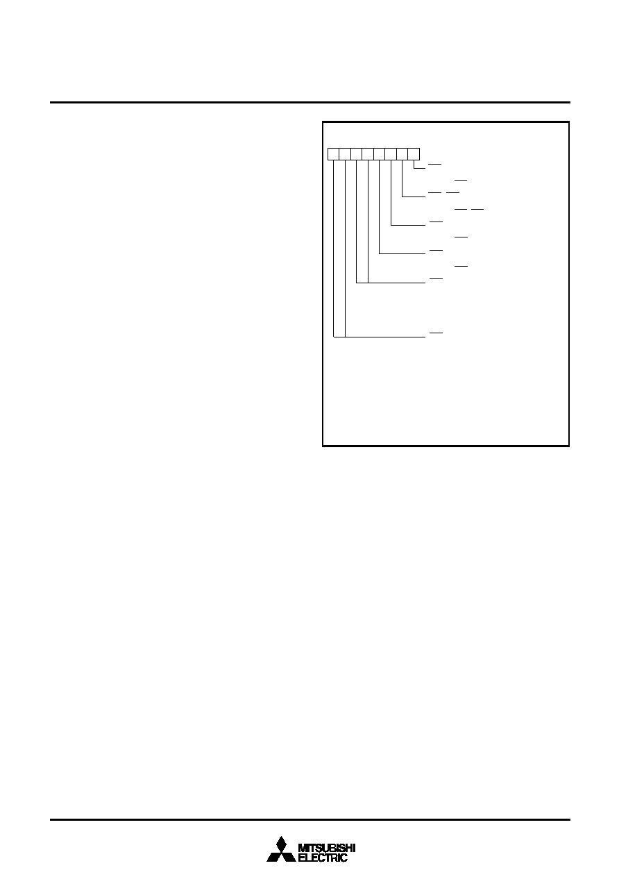
Fig. 87 Chip select control register bit configuration
Address
6216
CS0 function select bit (Note 1)
0 : Port P90 function
1 : CS0 output
CS4 function select bit
0 : Port P94 function
1 : CS4 output
CS1, CS2 function select bit (Note 2)
0 : Port P91, P92 function
1 : CS1, CS2 output or A20, A21 output
CS3 function select bit (Note 2)
0 : Port P93 function
1 : CS3 output or A22 output
76543210
CS3 bus cycle select bits
b5 b4 In high-speed In low-speed
0 0 : 5-
φ access
Do not select.
0 1 : 4-
φ access
4-
φ access
1 0 : 3-
φ access
3-
φ access
1 1 : Do not select. 2-
φ access
CS4 bus cycle select bits
b7 b6 In high-speed In low-speed
0 0 : 5-
φ access
Do not select.
0 1 : 4-
φ access
4-
φ access
1 0 : 3-
φ access
3-
φ access
1 1 : Do not select. 2-
φ access
Notes 1 : At reset, bit 0 becomes “0” when the CNVss pin’s level is “L”;
bit 0 becomes “1” when the CNVss pin’s level is “H”.
2 : Bits 6 and 7 of chip select area register (address 6316) specify
whether the chip select signal or address is output.
Chip select control register
相關(guān)PDF資料 |
PDF描述 |
|---|---|
| M37754M8C-XXXHP | 16-BIT, MROM, 40 MHz, MICROCONTROLLER, PQFP100 |
| M37754S4CHP | 16-BIT, 40 MHz, MICROCONTROLLER, PQFP100 |
| M37754S4CHP | 16-BIT, 40 MHz, MICROCONTROLLER, PQFP100 |
| M37754M8C-XXXGP | 16-BIT, MROM, 40 MHz, MICROCONTROLLER, PQFP100 |
| M37777E9AGS | 16-BIT, UVPROM, 16 MHz, MICROCONTROLLER, CQCC100 |
相關(guān)代理商/技術(shù)參數(shù) |
參數(shù)描述 |
|---|---|
| M37754S4CHP | 制造商:RENESAS 制造商全稱(chēng):Renesas Technology Corp 功能描述:SINGLE-CHIP 16-BIT CMOS MICROCOMPUTER |
| M3775PR-H400CL | 制造商:Bonitron 功能描述:OVERVOLTAGE BRAKING RESISTOR |
| M3775RK-0.75A | 制造商:Bonitron 功能描述:OVERVOLTAGE BRAKING RESISTOR |
| M3775RK-C0.50A | 制造商:Bonitron 功能描述:OVERVOLTAGE BRAKING RESISTOR |
| M3775RK-C0.50B | 制造商:Bonitron 功能描述:OVERVOLTAGE BRAKING RESISTOR |
發(fā)布緊急采購(gòu),3分鐘左右您將得到回復(fù)。