- 您現(xiàn)在的位置:買(mǎi)賣(mài)IC網(wǎng) > PDF目錄45036 > M37549G1-XXXFP 8-BIT, MROM, 8 MHz, MICROCONTROLLER, PDSO24 PDF資料下載
參數(shù)資料
| 型號(hào): | M37549G1-XXXFP |
| 元件分類(lèi): | 微控制器/微處理器 |
| 英文描述: | 8-BIT, MROM, 8 MHz, MICROCONTROLLER, PDSO24 |
| 封裝: | 5.30 X 10.10 MM, 0.80 MM PITCH, PLASTIC, SSOP-24 |
| 文件頁(yè)數(shù): | 31/84頁(yè) |
| 文件大?。?/td> | 1378K |
| 代理商: | M37549G1-XXXFP |
第1頁(yè)第2頁(yè)第3頁(yè)第4頁(yè)第5頁(yè)第6頁(yè)第7頁(yè)第8頁(yè)第9頁(yè)第10頁(yè)第11頁(yè)第12頁(yè)第13頁(yè)第14頁(yè)第15頁(yè)第16頁(yè)第17頁(yè)第18頁(yè)第19頁(yè)第20頁(yè)第21頁(yè)第22頁(yè)第23頁(yè)第24頁(yè)第25頁(yè)第26頁(yè)第27頁(yè)第28頁(yè)第29頁(yè)第30頁(yè)當(dāng)前第31頁(yè)第32頁(yè)第33頁(yè)第34頁(yè)第35頁(yè)第36頁(yè)第37頁(yè)第38頁(yè)第39頁(yè)第40頁(yè)第41頁(yè)第42頁(yè)第43頁(yè)第44頁(yè)第45頁(yè)第46頁(yè)第47頁(yè)第48頁(yè)第49頁(yè)第50頁(yè)第51頁(yè)第52頁(yè)第53頁(yè)第54頁(yè)第55頁(yè)第56頁(yè)第57頁(yè)第58頁(yè)第59頁(yè)第60頁(yè)第61頁(yè)第62頁(yè)第63頁(yè)第64頁(yè)第65頁(yè)第66頁(yè)第67頁(yè)第68頁(yè)第69頁(yè)第70頁(yè)第71頁(yè)第72頁(yè)第73頁(yè)第74頁(yè)第75頁(yè)第76頁(yè)第77頁(yè)第78頁(yè)第79頁(yè)第80頁(yè)第81頁(yè)第82頁(yè)第83頁(yè)第84頁(yè)
Rev.2.02
Mar 31, 2009
Page 37 of 81
REJ03B0202-0202
7549 Group
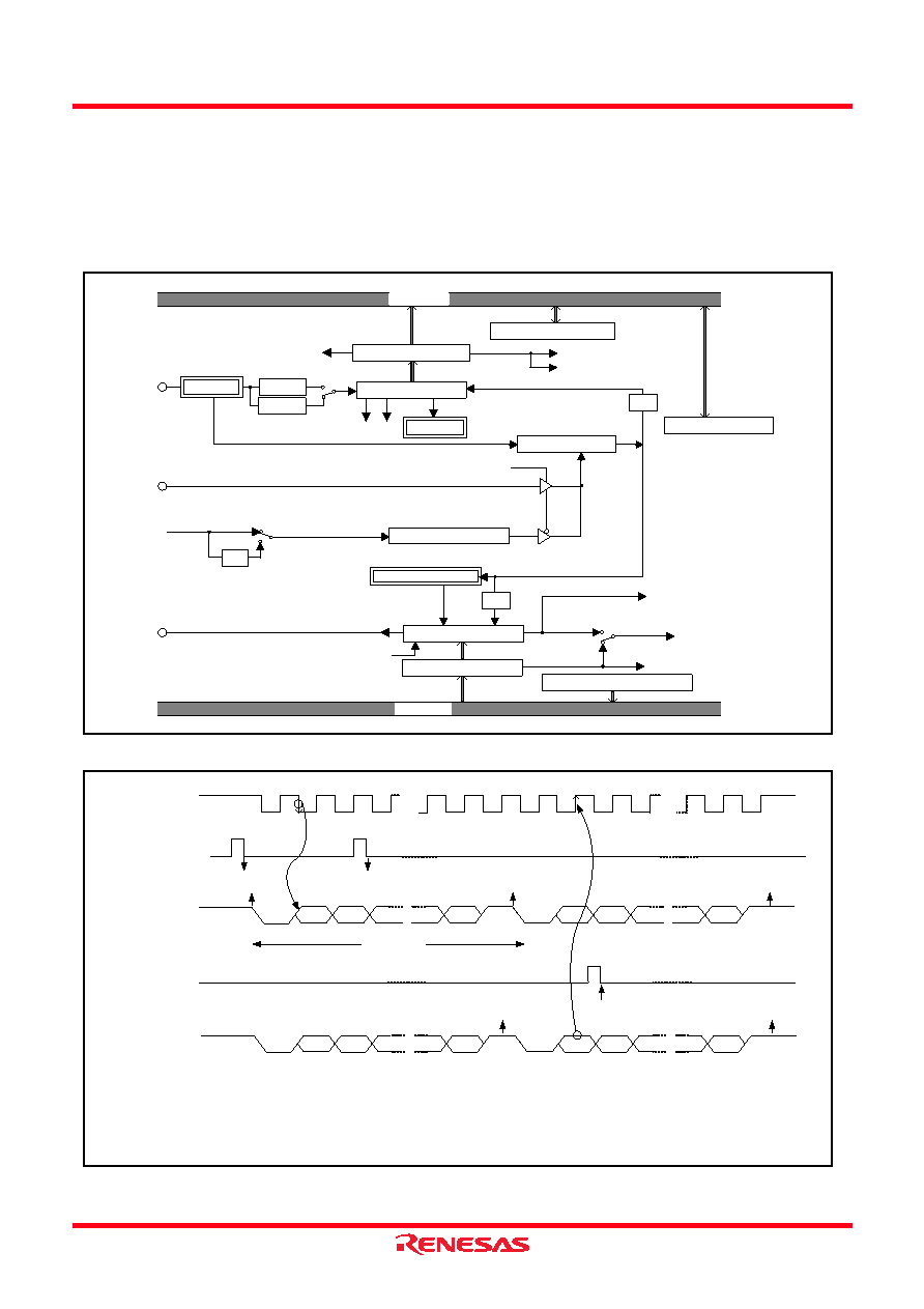
(2) Asynchronous Serial I/O (UART) Mode
Clock asynchronous serial I/O mode (UART) can be selected by
clearing the serial I/O mode selection bit of the serial I/O control
register to “0”.
Eight serial data transfer formats can be selected, and the transfer
formats used by a transmitter and receiver must be identical.
The transmit and receive shift registers each have a buffer, but
the two buffers have the same address in memory. Since the shift
register cannot be written to or read from directly, transmit data
is written to the transmit buffer register, and receive data is read
from the receive buffer register.
The transmit buffer register can also hold the next data to be
transmitted, and the receive buffer register can hold a character
while the next character is being received.
Fig 47. Block diagram of UART serial I/O
Fig 48. Operation of UART serial I/O function
1/4
OE
PE FE
1/16
Data bus
Receive buffer register
Address 001816
Receive shift register
Receive buffer full flag (RBF)
Receive interrupt request (RI)
Baud rate generator
Frequency division ratio 1/(n+1)
Address 001C16
ST/SP/PA generator
Transmit buffer register
Transmit shift register
Address 001816
Transmit shift completion flag (TSC)
Transmit buffer empty flag (TBE)
Transmit interrupt request (TI)
Address 001916
ST detector
SP detector
UART control register
Address 001B16
Character length selection bit
Address 001A16
BRG count source selection bit
Transmit interrupt source selection bit
Serial I/O1 synchronous clock selection bit
Clock control circuit
Character length selection bit
7 bits
8 bits
Serial I/O1 status register
Serial I/O 1 control register
P06/SCLK
P04/RXD
P05/TXD
φSOURCE
TSC=0
TBE=1
RBF=0
TBE=0
RBF=1
TBE=1
TSC=1*
ST
D0
D1
SP
D0
D1
ST
SP
Transmit or receive clock
Transmit buffer
write signal
Serial output TXD
Receive buffer
read signal
Serial input RXD
* Generated at 2nd bit in 2-stop-bit mode
1 start bit
7 or 8 data bit
1 or 0 parity bit
1 or 2 stop bit (s)
Notes 1: Error flag detection occurs at the same time that the RBF flag becomes “1” (at 1st stop bit, during reception).
2: As the transmit interrupt (TI), when either the TBE or TSC flag becomes “1”, can be selected to occur depending on the setting of the transmit
interrupt source selection bit (TIC) of the serial I/O1 control register.
3: The receive interrupt (RI) is set when the RBF flag becomes “1”.
4: After data is written to the transmit buffer when TSC=1, 0.5 to 1.5 cycles of the data shift cycle is necessary until changing to TSC=0.
ST
D0
D1
SP
D0
D1
ST
SP
相關(guān)PDF資料 |
PDF描述 |
|---|---|
| M37549G3-XXXFP | 8-BIT, MROM, 8 MHz, MICROCONTROLLER, PDSO24 |
| M37560M8-XXXFP | 8-BIT, MROM, 8 MHz, MICROCONTROLLER, PQFP100 |
| M37560MF-XXXGP | 8-BIT, MROM, 8 MHz, MICROCONTROLLER, PQFP100 |
| M37641F8FP | 8-BIT, FLASH, 12 MHz, MICROCONTROLLER, PQFP80 |
| M37641M8-XXXFP | 8-BIT, MROM, 24 MHz, MICROCONTROLLER, PQFP80 |
相關(guān)代理商/技術(shù)參數(shù) |
參數(shù)描述 |
|---|---|
| M37549G2FP | 制造商:RENESAS 制造商全稱(chēng):Renesas Technology Corp 功能描述:SINGLE-CHIP 8-BIT CMOS MICROCOMPUTER |
| M37549G2-XXXFP | 制造商:RENESAS 制造商全稱(chēng):Renesas Technology Corp 功能描述:SINGLE-CHIP 8-BIT CMOS MICROCOMPUTER |
| M37549G3FP | 制造商:RENESAS 制造商全稱(chēng):Renesas Technology Corp 功能描述:SINGLE-CHIP 8-BIT CMOS MICROCOMPUTER |
| M37549G3-XXXFP | 制造商:RENESAS 制造商全稱(chēng):Renesas Technology Corp 功能描述:SINGLE-CHIP 8-BIT CMOS MICROCOMPUTER |
| M37549RLSS | 制造商:RENESAS 制造商全稱(chēng):Renesas Technology Corp 功能描述:SINGLE-CHIP 8-BIT CMOS MICROCOMPUTER |
發(fā)布緊急采購(gòu),3分鐘左右您將得到回復(fù)。