- 您現(xiàn)在的位置:買賣IC網(wǎng) > PDF目錄45034 > M37531M4-XXXGP 8-BIT, MROM, 8 MHz, MICROCONTROLLER, PQFP32 PDF資料下載
參數(shù)資料
| 型號(hào): | M37531M4-XXXGP |
| 元件分類: | 微控制器/微處理器 |
| 英文描述: | 8-BIT, MROM, 8 MHz, MICROCONTROLLER, PQFP32 |
| 封裝: | 7 X 7 MM, 0.80 MM PITCH, PLASTIC, LQFP-32 |
| 文件頁(yè)數(shù): | 96/216頁(yè) |
| 文件大小: | 1400K |
| 代理商: | M37531M4-XXXGP |
第1頁(yè)第2頁(yè)第3頁(yè)第4頁(yè)第5頁(yè)第6頁(yè)第7頁(yè)第8頁(yè)第9頁(yè)第10頁(yè)第11頁(yè)第12頁(yè)第13頁(yè)第14頁(yè)第15頁(yè)第16頁(yè)第17頁(yè)第18頁(yè)第19頁(yè)第20頁(yè)第21頁(yè)第22頁(yè)第23頁(yè)第24頁(yè)第25頁(yè)第26頁(yè)第27頁(yè)第28頁(yè)第29頁(yè)第30頁(yè)第31頁(yè)第32頁(yè)第33頁(yè)第34頁(yè)第35頁(yè)第36頁(yè)第37頁(yè)第38頁(yè)第39頁(yè)第40頁(yè)第41頁(yè)第42頁(yè)第43頁(yè)第44頁(yè)第45頁(yè)第46頁(yè)第47頁(yè)第48頁(yè)第49頁(yè)第50頁(yè)第51頁(yè)第52頁(yè)第53頁(yè)第54頁(yè)第55頁(yè)第56頁(yè)第57頁(yè)第58頁(yè)第59頁(yè)第60頁(yè)第61頁(yè)第62頁(yè)第63頁(yè)第64頁(yè)第65頁(yè)第66頁(yè)第67頁(yè)第68頁(yè)第69頁(yè)第70頁(yè)第71頁(yè)第72頁(yè)第73頁(yè)第74頁(yè)第75頁(yè)第76頁(yè)第77頁(yè)第78頁(yè)第79頁(yè)第80頁(yè)第81頁(yè)第82頁(yè)第83頁(yè)第84頁(yè)第85頁(yè)第86頁(yè)第87頁(yè)第88頁(yè)第89頁(yè)第90頁(yè)第91頁(yè)第92頁(yè)第93頁(yè)第94頁(yè)第95頁(yè)當(dāng)前第96頁(yè)第97頁(yè)第98頁(yè)第99頁(yè)第100頁(yè)第101頁(yè)第102頁(yè)第103頁(yè)第104頁(yè)第105頁(yè)第106頁(yè)第107頁(yè)第108頁(yè)第109頁(yè)第110頁(yè)第111頁(yè)第112頁(yè)第113頁(yè)第114頁(yè)第115頁(yè)第116頁(yè)第117頁(yè)第118頁(yè)第119頁(yè)第120頁(yè)第121頁(yè)第122頁(yè)第123頁(yè)第124頁(yè)第125頁(yè)第126頁(yè)第127頁(yè)第128頁(yè)第129頁(yè)第130頁(yè)第131頁(yè)第132頁(yè)第133頁(yè)第134頁(yè)第135頁(yè)第136頁(yè)第137頁(yè)第138頁(yè)第139頁(yè)第140頁(yè)第141頁(yè)第142頁(yè)第143頁(yè)第144頁(yè)第145頁(yè)第146頁(yè)第147頁(yè)第148頁(yè)第149頁(yè)第150頁(yè)第151頁(yè)第152頁(yè)第153頁(yè)第154頁(yè)第155頁(yè)第156頁(yè)第157頁(yè)第158頁(yè)第159頁(yè)第160頁(yè)第161頁(yè)第162頁(yè)第163頁(yè)第164頁(yè)第165頁(yè)第166頁(yè)第167頁(yè)第168頁(yè)第169頁(yè)第170頁(yè)第171頁(yè)第172頁(yè)第173頁(yè)第174頁(yè)第175頁(yè)第176頁(yè)第177頁(yè)第178頁(yè)第179頁(yè)第180頁(yè)第181頁(yè)第182頁(yè)第183頁(yè)第184頁(yè)第185頁(yè)第186頁(yè)第187頁(yè)第188頁(yè)第189頁(yè)第190頁(yè)第191頁(yè)第192頁(yè)第193頁(yè)第194頁(yè)第195頁(yè)第196頁(yè)第197頁(yè)第198頁(yè)第199頁(yè)第200頁(yè)第201頁(yè)第202頁(yè)第203頁(yè)第204頁(yè)第205頁(yè)第206頁(yè)第207頁(yè)第208頁(yè)第209頁(yè)第210頁(yè)第211頁(yè)第212頁(yè)第213頁(yè)第214頁(yè)第215頁(yè)第216頁(yè)
8
8-4
INPUT/OUTPUT PORTS AND PIN FUNCTIONS
32182 Group User’s Manual (Rev.1.0)
8.2 Selecting Pin Functions
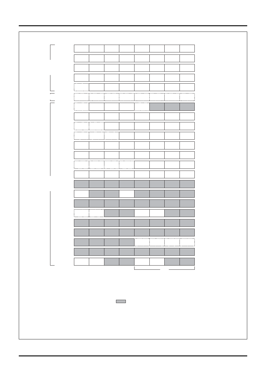
Figure 8.2.1 Input/Output Ports and Pin Function Assignments
0
1
2
3
4
5
6
7
P0
P1
P2
P3
P4
P5
P6
P7
P8
P9
P10
P11
P12
P13
P14
P15
P16
P17
P18
P19
P20
P21
P22
Input/output
port operation
mode setting
(Reserved)
CPU operation
mode settings
(Note 1)
DB0
DB1
DB2
DB3
DB4
DB5
DB6
DB7
DB8
DB9
DB10
DB11
DB12
DB13
DB14
DB15
A23
A24
A25
A26
A27
A28
A29
A30
A15
A16
A17
A18
A19
A20
A21
A22
TO16
TO17
TO18
TO19
TO20
TO9 /
TO10 /
TO8
TO11
TO12
TO13
TO14
TO15
TXD3(Note 2) CTX1(Note 2)
A11 /
A12 /
CTX0
CRX0
CTX1
CRX1
CS2#
CS3#
CS2#(Note 2)CS3#(Note 2)
TO0
TO1
TO2
TO3
TO4
TO5
TO6
TO7
TCLK0
TCLK1
TCLK2
TCLK3
TIN0
TIN1
TIN2
TIN3
TIN4
TIN5
TIN6
TIN7
TO21
TO22
TO23
TO24
TO25
TO26
TO27
TO28
TO29
TO30
TO31
TO32
TO33
TO34
TO35
TO36
TIN33/
TIN26
TIN27
TIN28
TIN29
TIN30
TIN31
TIN32
PWMOFF2
TXD4
RXD4
TXD5
RXD5
TO37
TO38
TO39
TO40
TO41
TO42
TO43
TO44
TIN8
TIN9
TIN10
TIN11
TIN12
TIN13
TIN14
TIN15
TIN24
TIN25
TXD2
RXD2
TXD3
RXD3
MOD0
MOD1
SCLKI0 /
SCLKI1 /
TXD0
RXD0
TXD1
RXD1
(Note 3)
SCLKO0
SCLKO1
BLW# /
BHW# /
RD#
CS0#
CS1#
A13
A14
BLE#
BHE#
BCLK /
WAIT#
HREQ#
HACK#
RTDTXD RTDRXD
RTDACK
RTDCLK
WR#
SBI#
SCLKI4 /
SCLKI5 /
(P61)
(P62)
(P63)
(P67)
(Note 3)
SCLKO4
SCLKO5
TIN21 /
TIN22 /
TIN16
TIN17
TIN18
TIN19
TIN20
TIN23
RXD3
CRX1
Note 1: During processor mode, these ports are switched to function as extended external signal pins. During external extension
mode, only P41-P43 are switched to function as external bus interface pins. Other pins become input/output port pins
when reset, so that some of these pins, if needed, must be set to function as external bus interface pins.
Note 2: These are triple-function pins. Their desired output function must be selected using the peripheral output select register.
Note 3: These ports cannot be used for input/output port function. The SBI#, MOD0 and MOD1 pin input levels can be read from
these ports.
Note: No pins are available for those in shaded sections
. However, because internal circuits are included, make sure
the ports are set for low-level output when initialized (to prevent current from flowing in through the port). These pins exist
in only the 32180 and are nonexistent in the 32182. However, P223 is an input-only pin and internally pulled high, so that
there is no need to set it for output.
相關(guān)PDF資料 |
PDF描述 |
|---|---|
| M37531M4T-XXXGP | 8-BIT, MROM, 8 MHz, MICROCONTROLLER, PQFP32 |
| M37531M8-XXXFP | 8-BIT, MROM, 8 MHz, MICROCONTROLLER, PDSO36 |
| M37531M4T-XXXFP | 8-BIT, MROM, 8 MHz, MICROCONTROLLER, PDSO36 |
| M37531M4T-XXXGP | 8-BIT, MROM, 8 MHz, MICROCONTROLLER, PQFP32 |
| M37531E4V-XXXGP | 8-BIT, OTPROM, 8 MHz, MICROCONTROLLER, PQFP32 |
相關(guān)代理商/技術(shù)參數(shù) |
參數(shù)描述 |
|---|---|
| M37531RSS | 制造商:Mitsubishi Electric 功能描述: |
| M37531T-ADS | 制造商:RENESAS 制造商全稱:Renesas Technology Corp 功能描述:Temporary Target Board |
| M37532E8FP | 制造商:MITSUBISHI 制造商全稱:Mitsubishi Electric Semiconductor 功能描述:SINGLE-CHIP 8-BIT CMOS MICROCOMPUTER |
| M37532M4 | 制造商:MITSUBISHI 制造商全稱:Mitsubishi Electric Semiconductor 功能描述:SINGLE-CHIP 8-BIT CMOS MICROCOMPUTER |
| M37532M4-A17GP | 制造商:MITSUBISHI 制造商全稱:Mitsubishi Electric Semiconductor 功能描述:SINGLE-CHIP 8-BIT CMOS MICROCOMPUTER |
發(fā)布緊急采購(gòu),3分鐘左右您將得到回復(fù)。