- 您現(xiàn)在的位置:買賣IC網(wǎng) > PDF目錄370844 > M37471M4 (Mitsubishi Electric Corporation) SINGLE-CHIP 8-BIT CMOS MICROCOMPUTER PDF資料下載
參數(shù)資料
| 型號: | M37471M4 |
| 廠商: | Mitsubishi Electric Corporation |
| 英文描述: | SINGLE-CHIP 8-BIT CMOS MICROCOMPUTER |
| 中文描述: | 單芯片8位CMOS微機 |
| 文件頁數(shù): | 11/46頁 |
| 文件大小: | 646K |
| 代理商: | M37471M4 |
第1頁第2頁第3頁第4頁第5頁第6頁第7頁第8頁第9頁第10頁當(dāng)前第11頁第12頁第13頁第14頁第15頁第16頁第17頁第18頁第19頁第20頁第21頁第22頁第23頁第24頁第25頁第26頁第27頁第28頁第29頁第30頁第31頁第32頁第33頁第34頁第35頁第36頁第37頁第38頁第39頁第40頁第41頁第42頁第43頁第44頁第45頁第46頁
11
7470/7471 Group
SINGLE-CHIP 8-BIT CMOS MICROCOMPUTER
MITSUBISHI MICROCOMPUTERS
INTERRUPTS
Interrupts can be caused by 12 different sources consisting of five
external, six internal, and one software sources.
Interrupts are vectored interrupts with priorities shown in Table 1.
Reset is also included in the table because its operation is similar
to an interrupt.
When an interrupt is accepted, the registers are pushed, interrupt
disable flag I is set, and the program jumps to the address speci-
fied in the vector table. The interrupt request bit is cleared
automatically. The reset and BRK instruction interrupt can never
be disabled. Other interrupts are disabled when the interrupt dis-
able flag is set.
All interrupts except the BRK instruction interrupt have an interrupt
request bit and an interrupt enable bit. The interrupt request bits
are in interrupt request registers 1 and 2 and the interrupt enable
bits are in interrupt control registers 1 and 2. External interrupts
INT
0
and INT
1
can be asserted on either the falling or rising edge
as set in the edge polarity selection register. When “0” is set to this
register, the interrupt is activated on the falling edge; when “1” is
set to the register, the interrupt is activated on the rising edge.
When the device is put into power-down state by the STP instruc-
tion or the WIT instruction, if bit 5 in the edge polarity selection
register is “1”, the INT
1
interrupt becomes a key on wake up inter-
rupt. When a key on wake up interrupt is valid, an interrupt request
is generated by applying the “L” level to any pin in port P0. In this
case, the port used for interrupt must have been set for the input
mode.
If bit 5 in the edge polarity selection register is “0” when the device
is in power-down state, the INT
1
interrupt is selected. Also, if bit 5
in the edge polarity selection register is set to “1” when the device
is not in a power-down state, neither key on wake up interrupt re-
quest nor INT
1
interrupt request is generated.
The CNTR
0
/CNTR
1
interrupts function in the same as INT
0
and
INT
1
. The interrupt input pin can be specified for either CNTR
0
or
CNTR
1
pin by setting bit 4 in the edge polarity selection register.
Figure 4 shows the structure of the edge polarity selection regis-
ter, interrupt request registers 1 and 2, and interrupt control
registers 1 and 2.
Interrupts other than the BRK instruction interrupt and reset are
accepted when the interrupt enable bit is “1”, interrupt request bit
is “1”, and the interrupt disable flag is “0”. The interrupt request bit
can be reset with a program, but not set. The interrupt enable bit
can be set and reset with a program.
Reset is treated as a non-maskable interrupt with the highest pri-
ority. Figure 5 shows interrupts control.
Interrupt source
RESET
INT
0
interrupt
INT
1
interrupt or key on wake up interrupt
CNTR
0
interrupt or CNTR
1
interrupt
Timer 1 interrupt
Timer 2 interrupt
Timer 3 interrupt
Timer 4 interrupt
Serial I/O interrupt
A-D conversion completion interrupt
BRK instruction interrupt
Priority
1
2
3
4
5
6
7
8
9
10
11
Vector addresses
FFFF
16
, FFFE
16
FFFD
16
, FFFC
16
FFFB
16
, FFFA
16
FFF9
16
, FFF8
16
FFF7
16
, FFF6
16
FFF5
16
, FFF4
16
FFF3
16
, FFF2
16
FFF1
16
, FFF0
FFEF
16
, FFEE
16
FFED
16
, FFEC
16
FFEB
16
, FFEA
16
Remarks
Non-maskable
External interrupt (polarity programmable)
External interrupt (INT
1
is polarity programmable)
External interrupt (polarity programmable)
Non-maskable software interrupt
Table 1. Interrupt vector address and priority
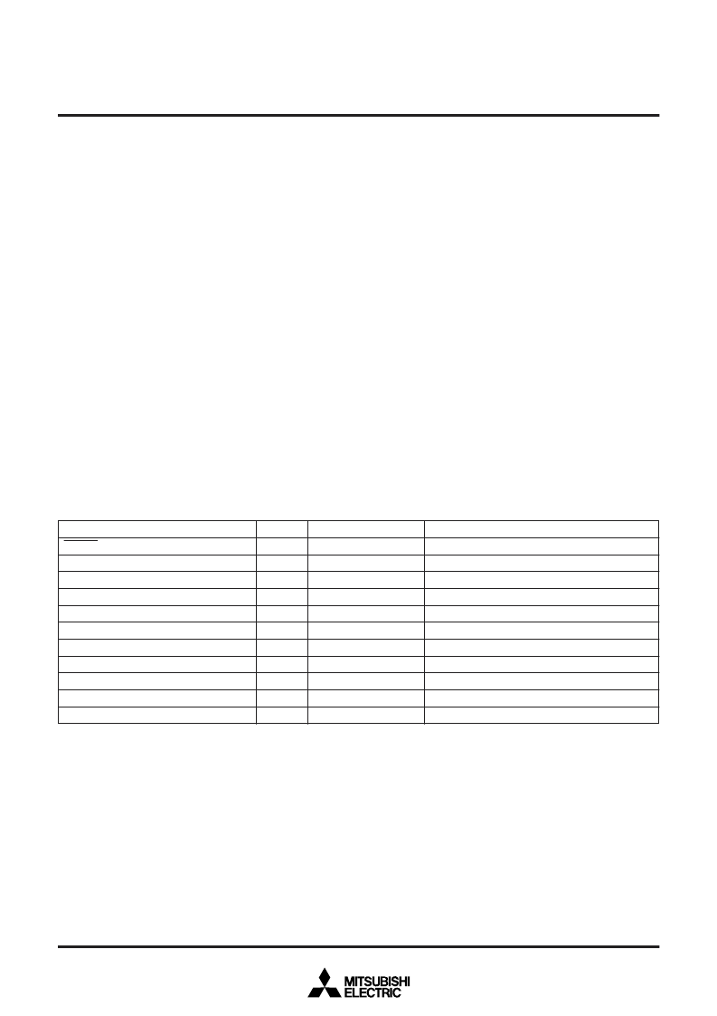
相關(guān)PDF資料 |
PDF描述 |
|---|---|
| M37471M4-XXXSP | SINGLE-CHIP 8-BIT CMOS MICROCOMPUTER |
| M37471M8 | SINGLE-CHIP 8-BIT CMOS MICROCOMPUTER |
| M37471M8-XXXFP | SINGLE-CHIP 8-BIT CMOS MICROCOMPUTER |
| M37471M8-XXXSP | SINGLE-CHIP 8-BIT CMOS MICROCOMPUTER |
| M37470 | Single Chip 8 Bits CMOS Microcomputer(8位單片機) |
相關(guān)代理商/技術(shù)參數(shù) |
參數(shù)描述 |
|---|---|
| M37471M4-214SP | 制造商:MITSUBISHI 制造商全稱:Mitsubishi Electric Semiconductor 功能描述:SINGLE-CHIP 8-BIT CMOS MICROCOMPUTER |
| M37471M4-425SP | 制造商:MITSUBISHI 制造商全稱:Mitsubishi Electric Semiconductor 功能描述:SINGLE-CHIP 8-BIT CMOS MICROCOMPUTER |
| M37471M4-468SP | 制造商:MITSUBISHI 制造商全稱:Mitsubishi Electric Semiconductor 功能描述:SINGLE-CHIP 8-BIT CMOS MICROCOMPUTER |
| M37471M4-833SP | 制造商:MITSUBISHI 制造商全稱:Mitsubishi Electric Semiconductor 功能描述:SINGLE-CHIP 8-BIT CMOS MICROCOMPUTER |
| M37471M4-XXXFP | 制造商:RENESAS 制造商全稱:Renesas Technology Corp 功能描述:SINGLE-CHIP 8-BIT CMOS MICROCOMPUTER |
發(fā)布緊急采購,3分鐘左右您將得到回復(fù)。