- 您現(xiàn)在的位置:買賣IC網(wǎng) > PDF目錄370842 > M37280MF-171SP (Mitsubishi Electric Corporation) SINGLE-CHIP 8-BIT CMOS MICROCOMPUTER with CLOSED CAPTION DECODER and ON-SCREEN DISPLAY CONTROLLER PDF資料下載
參數(shù)資料
| 型號(hào): | M37280MF-171SP |
| 廠商: | Mitsubishi Electric Corporation |
| 英文描述: | SINGLE-CHIP 8-BIT CMOS MICROCOMPUTER with CLOSED CAPTION DECODER and ON-SCREEN DISPLAY CONTROLLER |
| 中文描述: | 單芯片8位CMOS微機(jī)隱蔽字幕解碼器和屏幕顯示控制器 |
| 文件頁(yè)數(shù): | 7/178頁(yè) |
| 文件大小: | 1457K |
| 代理商: | M37280MF-171SP |
第1頁(yè)第2頁(yè)第3頁(yè)第4頁(yè)第5頁(yè)第6頁(yè)當(dāng)前第7頁(yè)第8頁(yè)第9頁(yè)第10頁(yè)第11頁(yè)第12頁(yè)第13頁(yè)第14頁(yè)第15頁(yè)第16頁(yè)第17頁(yè)第18頁(yè)第19頁(yè)第20頁(yè)第21頁(yè)第22頁(yè)第23頁(yè)第24頁(yè)第25頁(yè)第26頁(yè)第27頁(yè)第28頁(yè)第29頁(yè)第30頁(yè)第31頁(yè)第32頁(yè)第33頁(yè)第34頁(yè)第35頁(yè)第36頁(yè)第37頁(yè)第38頁(yè)第39頁(yè)第40頁(yè)第41頁(yè)第42頁(yè)第43頁(yè)第44頁(yè)第45頁(yè)第46頁(yè)第47頁(yè)第48頁(yè)第49頁(yè)第50頁(yè)第51頁(yè)第52頁(yè)第53頁(yè)第54頁(yè)第55頁(yè)第56頁(yè)第57頁(yè)第58頁(yè)第59頁(yè)第60頁(yè)第61頁(yè)第62頁(yè)第63頁(yè)第64頁(yè)第65頁(yè)第66頁(yè)第67頁(yè)第68頁(yè)第69頁(yè)第70頁(yè)第71頁(yè)第72頁(yè)第73頁(yè)第74頁(yè)第75頁(yè)第76頁(yè)第77頁(yè)第78頁(yè)第79頁(yè)第80頁(yè)第81頁(yè)第82頁(yè)第83頁(yè)第84頁(yè)第85頁(yè)第86頁(yè)第87頁(yè)第88頁(yè)第89頁(yè)第90頁(yè)第91頁(yè)第92頁(yè)第93頁(yè)第94頁(yè)第95頁(yè)第96頁(yè)第97頁(yè)第98頁(yè)第99頁(yè)第100頁(yè)第101頁(yè)第102頁(yè)第103頁(yè)第104頁(yè)第105頁(yè)第106頁(yè)第107頁(yè)第108頁(yè)第109頁(yè)第110頁(yè)第111頁(yè)第112頁(yè)第113頁(yè)第114頁(yè)第115頁(yè)第116頁(yè)第117頁(yè)第118頁(yè)第119頁(yè)第120頁(yè)第121頁(yè)第122頁(yè)第123頁(yè)第124頁(yè)第125頁(yè)第126頁(yè)第127頁(yè)第128頁(yè)第129頁(yè)第130頁(yè)第131頁(yè)第132頁(yè)第133頁(yè)第134頁(yè)第135頁(yè)第136頁(yè)第137頁(yè)第138頁(yè)第139頁(yè)第140頁(yè)第141頁(yè)第142頁(yè)第143頁(yè)第144頁(yè)第145頁(yè)第146頁(yè)第147頁(yè)第148頁(yè)第149頁(yè)第150頁(yè)第151頁(yè)第152頁(yè)第153頁(yè)第154頁(yè)第155頁(yè)第156頁(yè)第157頁(yè)第158頁(yè)第159頁(yè)第160頁(yè)第161頁(yè)第162頁(yè)第163頁(yè)第164頁(yè)第165頁(yè)第166頁(yè)第167頁(yè)第168頁(yè)第169頁(yè)第170頁(yè)第171頁(yè)第172頁(yè)第173頁(yè)第174頁(yè)第175頁(yè)第176頁(yè)第177頁(yè)第178頁(yè)
7
SINGLE-CHIP 8-BIT CMOS MICROCOMPUTER with CLOSED CAPTION DECODER
and ON-SCREEN DISPLAY CONTROLLER
M37280MF–XXXSP, M37280MK–XXXSP
M37280EKSP
MITSUBISHI MICROCOMPUTERS
PRELIMINARY
Notice: This is not a final specification.
Some paramentic limits are subject to change.
Rev. 1.0
V
CC
,
AV
CC
,
V
SS
CNV
SS
RESET
X
IN
X
OUT
P0
0
/
PWM4–
P0
2
/PWM6,
P0
3
/PWM7,
P0
4
/
PWM0–
P0
7
/PWM3
P10/OUT2,
P11/SCL1,
P12/SCL2,
P13/SDA1,
P14/SDA2,
P15/G0,
P16/INT3/
B0,
P17/S
IN
/R0
P2
0
–P2
3
P2
4
/AD3–
P2
6
/AD1
,
P2
7
/AD5
P3
0
/AD7,
P3
1
/AD8
P3
2
P4
0
/AD4,
P4
1
/INT2,
P4
2
/TIM2,
P4
3
/TIM3,
P4
4
/INT1,
P4
5
/S
OUT
,
P4
6
/S
CLK
P4
7
Input
Input
Input
Output
I/O
Output
I/O
Output
Output
Input
Input
I/O
Input
I/O
Input
Output
Input
Input
Input
Input
Output
I/O
Output
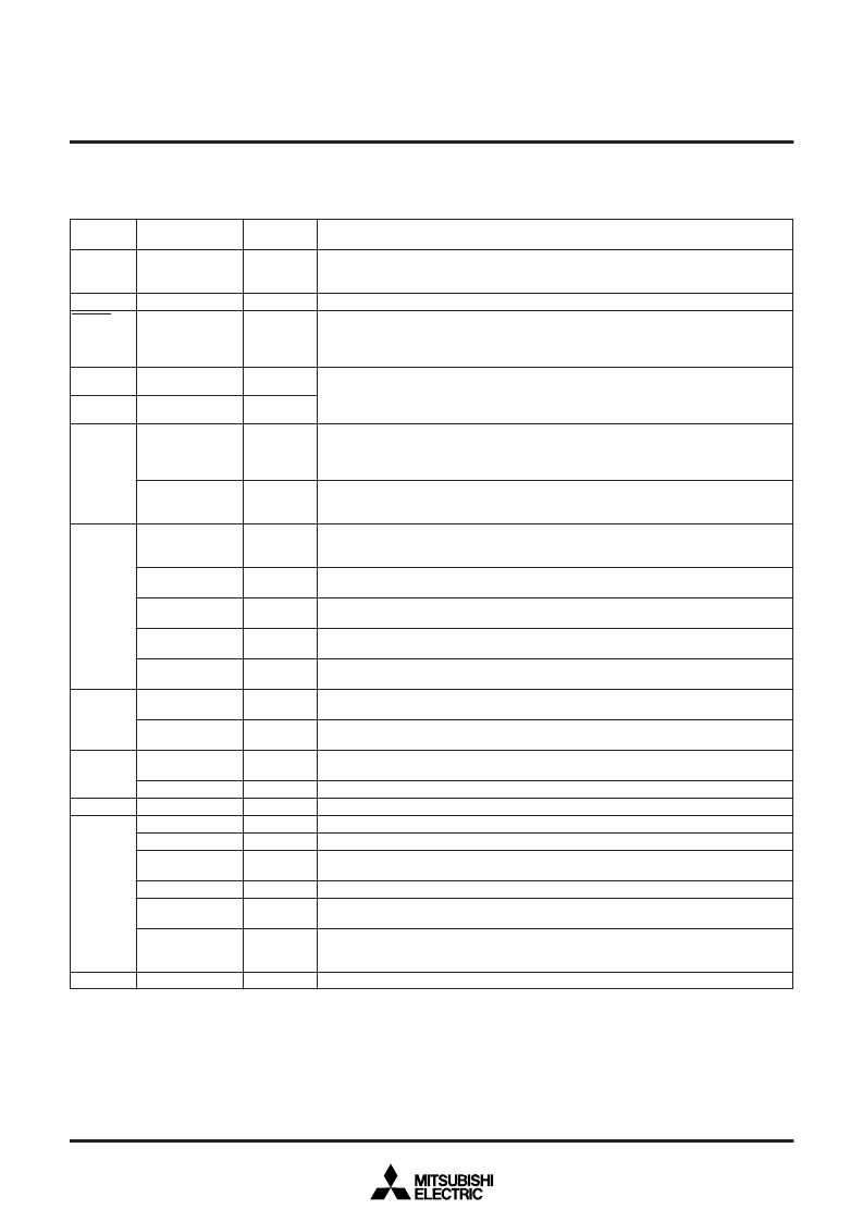
Apply voltage of 5 V ± 10 % (typical) to V
CC
and AV
CC
, and 0 V to V
SS
.
Connected to V
SS
.
To enter the reset state, the reset input pin must be kept at a LOW for 2
μ
s or more (under
normal V
CC
conditions).
If more time is needed for the quartz-crystal oscillator to stabilize, this LOW condition should
be maintained for the required time.
This chip has an internal clock generating circuit. To control generating frequency, an exter-
nal ceramic resonator or a quartz-crystal oscillator is connected between pins X
IN
and X
OUT
.
If an external clock is used, the clock source should be connected to the X
IN
pin and the
X
OUT
pin should be left open.
Port P0 is an 8-bit I/O port with direction register allowing each I/O bit to be individually
programmed as input or output. At reset, this port is set to input mode. The output structure
of P0
3
is CMOS output, that of P0
0
–P0
2
and P0
4
–P0
7
are N-channel open-drain output. See
notes at end of Table for full details of port P0 functions.
Pins P0
0
–P0
3
and P0
4
–P0
7
are also used as 8-bit PWM output pins PWM4–PWM7 and
PWM0–PWM3 respectively. The output structure of PWM0–PWM6 is N-channel open-drain
output. And the output structure of PWM7 is CMOS output.
Port P1 is an 8-bit I/O port and has basically the same functions as port P0. The output
structure of P1
0
and P1
5
–P1
7
is CMOS output, that of P1
1
–P1
4
is N-channel open-drain
output.
Pin P1
0
, P1
5
–P1
7
are also used as OSD output pins OUT2, G0, B0, R0, respectively. The
output structure is CMOS output.
Pin P1
1
–P1
4
are used as SCL1, SCL2, SDA1 and SDA2 respectively, when multi-master
I
2
C-BUS interface is used. The output structure is N-channel open-drain output.
Pin P1
6
is also used as extemal interrupt input pin INT3.
Pin P1
7
is also used as serial I/O data input pin S
IN
.
Port P2 is an 8-bit I/O port and has basically the same functions as port P0. The output
structure is CMOS output.
Pins P2
4
–P2
6
, P2
7
are also used as analog input pins AD3–AD1, AD5 respectively.
Ports P3
0
and P3
1
are 2-bit I/O ports and have basically the same functions as port P0. The
output structure is CMOS output.
Pins P3
0
, P3
1
are also used as analog input pins AD7, AD8 respectively.
Ports P3
2
is a 1-bit output port. The output structure is N-channel open-drain output.
Ports P4
0
–P4
6
are a 7-bit input port.
Pin P4
0
is also used as analog input pin AD4.
Pins P4
1
, P4
4
are also used as external interrupt input pins INT2, INT1.
Pins P4
2
and P4
3
are also used as external clock input pins TIM2, TIM3 respectively.
Pin P4
5
is used as serial I/O data output pin S
OUT
. The output structure is N-channel open-
drain output.
Pin P4
6
is used as serial I/O synchronous clock input/output pin S
CLK
. The output structure
is N-channel open-drain output.
Port P4
7
is a 1-bit output port. The output structure is N-channel open-drain output.
Pin
Name
Functions
Input/
Output
Power source
CNV
SS
Reset input
Clock input
Clock output
I/O port P0
8-bit PWM output
I/O port P1
OSD output
Multi-master
I
2
C-BUS interface
External interrupt
input
Serial I/O data
input
I/O port P2
Analog input
I/O port P3
Analog input
Output port P3
Input port P4
Analog input
External interrupt
input
External clock input
Serial I/O data
output
Serial I/O
synchronous clock
input/output
Output port P4
11. PIN DESCRIPTION
Table 11.1 Pin Description
相關(guān)PDF資料 |
PDF描述 |
|---|---|
| M37280MK-103SP | Oscillator; Frequency:15.36MHz; Frequency Tolerance:+/-100ppm; Load Capacitance:50pF; Supply Voltage:5V; Crystal Terminals:Surface Mount (SMD, SMT); Leaded Process Compatible:Yes; Mounting Type:Surface Mount RoHS Compliant: Yes |
| M37280MK-104SP | Oscillator; Frequency:16MHz; Frequency Tolerance:+/-100ppm; Load Capacitance:50pF; Supply Voltage:5V; Crystal Terminals:Surface Mount (SMD, SMT); Fundamental Mode:Parallel Load; Leaded Process Compatible:Yes RoHS Compliant: Yes |
| M37409M2 | SINGLE CHIP 8 BIT MICROCOMPUTER |
| M37409M2-XXXFP | SINGLE CHIP 8 BIT MICROCOMPUTER |
| M37409M2-XXXSP | SINGLE CHIP 8 BIT MICROCOMPUTER |
相關(guān)代理商/技術(shù)參數(shù) |
參數(shù)描述 |
|---|---|
| M37280MFH-XXXSP | 制造商:RENESAS 制造商全稱:Renesas Technology Corp 功能描述:SNGLE-CHIP 8-BIT CMOS MICROCOMPUTER with CLOSED CAPTION DECODER and ON-SCREEN DISPLAY CONTROLLER |
| M37280MF-XXXSP | 制造商:RENESAS 制造商全稱:Renesas Technology Corp 功能描述:SINGLE-CHIP 8-BIT CMOS MICROCOMPUTER with CLOSED CAPTION DECODER and ON-SCREEN DISPLAY CONTROLLER |
| M37280MK | 制造商:MITSUBISHI 制造商全稱:Mitsubishi Electric Semiconductor 功能描述:SINGLE-CHIP 8-BIT CMOS MICROCOMPUTER with CLOSED CAPTION DECODER and ON-SCREEN DISPLAY CONTROLLER |
| M37280MK-103SP | 制造商:MITSUBISHI 制造商全稱:Mitsubishi Electric Semiconductor 功能描述:SINGLE-CHIP 8-BIT CMOS MICROCOMPUTER with CLOSED CAPTION DECODER and ON-SCREEN DISPLAY CONTROLLER |
| M37280MK-104SP | 制造商:MITSUBISHI 制造商全稱:Mitsubishi Electric Semiconductor 功能描述:SINGLE-CHIP 8-BIT CMOS MICROCOMPUTER with CLOSED CAPTION DECODER and ON-SCREEN DISPLAY CONTROLLER |
發(fā)布緊急采購(gòu),3分鐘左右您將得到回復(fù)。