- 您現(xiàn)在的位置:買賣IC網(wǎng) > PDF目錄370842 > M37274MA-082SP (Mitsubishi Electric Corporation) SINGLE-CHIP 8-BIT CMOS MICROCOMPUTER with CLOSED CAPTION DECODER and ON-SCREEN DISPLAY CONTROLLER PDF資料下載
參數(shù)資料
| 型號: | M37274MA-082SP |
| 廠商: | Mitsubishi Electric Corporation |
| 英文描述: | SINGLE-CHIP 8-BIT CMOS MICROCOMPUTER with CLOSED CAPTION DECODER and ON-SCREEN DISPLAY CONTROLLER |
| 中文描述: | 單芯片8位CMOS微機隱蔽字幕解碼器和屏幕顯示控制器 |
| 文件頁數(shù): | 103/147頁 |
| 文件大小: | 2042K |
| 代理商: | M37274MA-082SP |
第1頁第2頁第3頁第4頁第5頁第6頁第7頁第8頁第9頁第10頁第11頁第12頁第13頁第14頁第15頁第16頁第17頁第18頁第19頁第20頁第21頁第22頁第23頁第24頁第25頁第26頁第27頁第28頁第29頁第30頁第31頁第32頁第33頁第34頁第35頁第36頁第37頁第38頁第39頁第40頁第41頁第42頁第43頁第44頁第45頁第46頁第47頁第48頁第49頁第50頁第51頁第52頁第53頁第54頁第55頁第56頁第57頁第58頁第59頁第60頁第61頁第62頁第63頁第64頁第65頁第66頁第67頁第68頁第69頁第70頁第71頁第72頁第73頁第74頁第75頁第76頁第77頁第78頁第79頁第80頁第81頁第82頁第83頁第84頁第85頁第86頁第87頁第88頁第89頁第90頁第91頁第92頁第93頁第94頁第95頁第96頁第97頁第98頁第99頁第100頁第101頁第102頁當(dāng)前第103頁第104頁第105頁第106頁第107頁第108頁第109頁第110頁第111頁第112頁第113頁第114頁第115頁第116頁第117頁第118頁第119頁第120頁第121頁第122頁第123頁第124頁第125頁第126頁第127頁第128頁第129頁第130頁第131頁第132頁第133頁第134頁第135頁第136頁第137頁第138頁第139頁第140頁第141頁第142頁第143頁第144頁第145頁第146頁第147頁
103
SINGLE-CHIP 8-BIT CMOS MICROCOMPUTER with CLOSED CAPTION DECODER
and ON-SCREEN DISPLAY CONTROLLER
M37274EFSP
PRELIMINARY
Notice: This is not a final specification.
Some paramentic limits are subject to change.
MITSUBISHI MICROCOMPUTERS
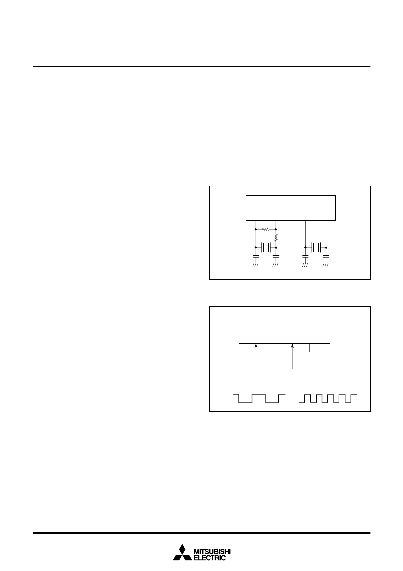
CLOCK GENERATING CIRCUIT
The M37274EFSP has 2 built-in oscillation circuits. An oscillation
circuit can be formed by connecting a resonator between X
IN
and
X
OUT
(X
CIN
and X
COUT
). Use the circuit constants in accordance with
the resonator manufacturer’s recommended values. No external re-
sistor is needed between X
IN
and X
OUT
since a feed-back resistor
exists on-chip. However, an external feed-back resistor is needed
between X
CIN
and X
COUT
. When using X
CIN
-X
COUT
as sub-clock,
clear bits 5 and 4 of the clock source control register to “0.” To supply
a clock signal externally, input it to the X
IN
(X
CIN
) pin and make the
X
OUT
(X
COUT
) pin open. When not using X
CIN
clock, connect the
X
CIN
to V
SS
and make the X
COUT
pin open.
After reset has completed, the internal clock
φ
is half the frequency of
X
IN
. Immediately after poweron, both the X
IN
and X
CIN
clock start
oscillating. To set the internal clock
φ
to low-speed operation mode,
set bit 7 of the CPU mode register (address 00FB
16
) to “1.”
Oscillation Control
(1) Stop mode
The built-in clock generating circuit is shown in Figure 95. When the
STP instruction is executed, the internal clock
φ
stops at HIGH. At
the same time, timers 3 and 4 are connected by hardware and “FF
16
”
is set in timer 3 and “07
16
” is set in timer 4. Select f(X
IN
)/16 or f(X
CIN
)/
16 as the timer 3 count source (set both bit 0 of the timer mode
register 2 and bit 6 at address 00C7
16
to “0” before the execution of
the STP instruction). Moreover, set the timer 3 and timer 4 interrupt
enable bits to disabled (“0”) before execution of the STP instruction.
The oscillator restarts when external interrupt is accepted. However,
the internal clock
φ
keeps its “H” level until timer 4 overflows, allow-
ing time for oscillation stabilization when a ceramic resonator or a
quartz-crystal oscillator is used.
(2) Wait mode
When the WIT instruction is executed, the internal clock
φ
stops in
the “H” level but the oscillator continues running. This wait state is
released at reset or when an interrupt is accepted (Note). Since the
oscillator does not stop, the next instruction can be executed at once.
Note:
In the wait mode, the following interrupts are invalid.
(1) V
SYNC
interrupt
(2) OSD interrupt
(3) Timers 1 and 2 interrupts using TIM2 pin input as count
source
(4) Timer 3 interrupt using TIM3 pin input as count source
(5) Data slicer interrupt
(6) Multi-master I
2
C-BUS interface interrupt
(7) f(X
IN
)/4096 interrupt
(8) All timer interrupts using f(X
IN
)/2 or f(X
CIN
)/2 as count source
(9) All timer interrupts using f(X
IN
)/4096 or f(X
CIN
)/4096 as
count source
(10) A-D conversion interrupt
Fig. 107. Ceramic Resonator Circuit Example
Fig. 108. External Clock Input Circuit Example
(3) Low-Speed Mode
If the internal clock is generated from the sub-clock (X
CIN
), a low
power consumption operation can be realized by stopping only the
main clock X
IN
. To stop the main clock, set bit 6 (CM
6
) of the CPU
mode register (00FB
16
) to “1.” When the main clock X
IN
is restarted,
the program must allow enough time to for oscillation to stabilize.
Note that in low-power-consumption mode the X
CIN
-X
COUT
drivability
can be reduced, allowing even lower power consumption. To reduce
the X
CIN
-X
COUT
drivability, clear bit 5 (CM
5
) of the CPU mode regis-
ter (00FB
16
) to “0.” At reset, this bit is set to “1” and strong drivability
is selected to help the oscillation to start. When an STP instruction is
executed, set this bit to “1” by software before executing.
X
CIN
X
IN
C
CIN
M37274EFSP
X
COUT
R
f
R
d
C
COUT
X
OUT
C
IN
C
OUT
X
CIN
M37274EFSP
External oscillation
circuit or external
pulse
X
COUT
X
IN
X
OUT
Open
Open
External oscillation
circuit
Vcc
Vss
Vcc
Vss
相關(guān)PDF資料 |
PDF描述 |
|---|---|
| M37274MA-084SP | SINGLE-CHIP 8-BIT CMOS MICROCOMPUTER with CLOSED CAPTION DECODER and ON-SCREEN DISPLAY CONTROLLER |
| M37280MK-114SP | Oscillator; Frequency:16.384MHz; Frequency Tolerance:+/-100ppm; Load Capacitance:50pF; Supply Voltage:5V; Crystal Terminals:Surface Mount (SMD, SMT); Leaded Process Compatible:Yes; Mounting Type:Surface Mount RoHS Compliant: Yes |
| M37280MK-206SP | SINGLE-CHIP 8-BIT CMOS MICROCOMPUTER with CLOSED CAPTION DECODER and ON-SCREEN DISPLAY CONTROLLER |
| M37280EKSP | Single Chip 8 Bits Microcomputer(8位單片機) |
| M37280MF | Single Chip 8 Bits Microcomputer(8位單片機) |
相關(guān)代理商/技術(shù)參數(shù) |
參數(shù)描述 |
|---|---|
| M37274MA-084SP | 制造商:MITSUBISHI 制造商全稱:Mitsubishi Electric Semiconductor 功能描述:SINGLE-CHIP 8-BIT CMOS MICROCOMPUTER with CLOSED CAPTION DECODER and ON-SCREEN DISPLAY CONTROLLER |
| M37274MA-XXXSP | 制造商:RENESAS 制造商全稱:Renesas Technology Corp 功能描述:SINGLE-CHIP 8-BIT CMOS MICROCOMPUTER with CLOSED CAPTION DECODER and ON-SCREEN DISPLAY CONTROLLER |
| M37276MF248SP | 制造商:MITSUBISHI 功能描述:* |
| M37276MF2575P | 制造商:MITSUBISHI 功能描述:* |
| M37276MF260SP | 制造商:MITSUBISHI 功能描述:* |
發(fā)布緊急采購,3分鐘左右您將得到回復(fù)。