- 您現(xiàn)在的位置:買(mǎi)賣IC網(wǎng) > PDF目錄45028 > M3455AG8-XXXFP 4-BIT, OTPROM, 6 MHz, MICROCONTROLLER, PQFP52 PDF資料下載
參數(shù)資料
| 型號(hào): | M3455AG8-XXXFP |
| 元件分類: | 微控制器/微處理器 |
| 英文描述: | 4-BIT, OTPROM, 6 MHz, MICROCONTROLLER, PQFP52 |
| 封裝: | 10 X 10 MM, 0.65 MM PITCH, PLASTIC, LQFP-52 |
| 文件頁(yè)數(shù): | 107/150頁(yè) |
| 文件大?。?/td> | 1818K |
| 代理商: | M3455AG8-XXXFP |
第1頁(yè)第2頁(yè)第3頁(yè)第4頁(yè)第5頁(yè)第6頁(yè)第7頁(yè)第8頁(yè)第9頁(yè)第10頁(yè)第11頁(yè)第12頁(yè)第13頁(yè)第14頁(yè)第15頁(yè)第16頁(yè)第17頁(yè)第18頁(yè)第19頁(yè)第20頁(yè)第21頁(yè)第22頁(yè)第23頁(yè)第24頁(yè)第25頁(yè)第26頁(yè)第27頁(yè)第28頁(yè)第29頁(yè)第30頁(yè)第31頁(yè)第32頁(yè)第33頁(yè)第34頁(yè)第35頁(yè)第36頁(yè)第37頁(yè)第38頁(yè)第39頁(yè)第40頁(yè)第41頁(yè)第42頁(yè)第43頁(yè)第44頁(yè)第45頁(yè)第46頁(yè)第47頁(yè)第48頁(yè)第49頁(yè)第50頁(yè)第51頁(yè)第52頁(yè)第53頁(yè)第54頁(yè)第55頁(yè)第56頁(yè)第57頁(yè)第58頁(yè)第59頁(yè)第60頁(yè)第61頁(yè)第62頁(yè)第63頁(yè)第64頁(yè)第65頁(yè)第66頁(yè)第67頁(yè)第68頁(yè)第69頁(yè)第70頁(yè)第71頁(yè)第72頁(yè)第73頁(yè)第74頁(yè)第75頁(yè)第76頁(yè)第77頁(yè)第78頁(yè)第79頁(yè)第80頁(yè)第81頁(yè)第82頁(yè)第83頁(yè)第84頁(yè)第85頁(yè)第86頁(yè)第87頁(yè)第88頁(yè)第89頁(yè)第90頁(yè)第91頁(yè)第92頁(yè)第93頁(yè)第94頁(yè)第95頁(yè)第96頁(yè)第97頁(yè)第98頁(yè)第99頁(yè)第100頁(yè)第101頁(yè)第102頁(yè)第103頁(yè)第104頁(yè)第105頁(yè)第106頁(yè)當(dāng)前第107頁(yè)第108頁(yè)第109頁(yè)第110頁(yè)第111頁(yè)第112頁(yè)第113頁(yè)第114頁(yè)第115頁(yè)第116頁(yè)第117頁(yè)第118頁(yè)第119頁(yè)第120頁(yè)第121頁(yè)第122頁(yè)第123頁(yè)第124頁(yè)第125頁(yè)第126頁(yè)第127頁(yè)第128頁(yè)第129頁(yè)第130頁(yè)第131頁(yè)第132頁(yè)第133頁(yè)第134頁(yè)第135頁(yè)第136頁(yè)第137頁(yè)第138頁(yè)第139頁(yè)第140頁(yè)第141頁(yè)第142頁(yè)第143頁(yè)第144頁(yè)第145頁(yè)第146頁(yè)第147頁(yè)第148頁(yè)第149頁(yè)第150頁(yè)
Rev.1.02
Nov 26, 2008
Page 4 of 146
REJ03B0224-0102
455A Group
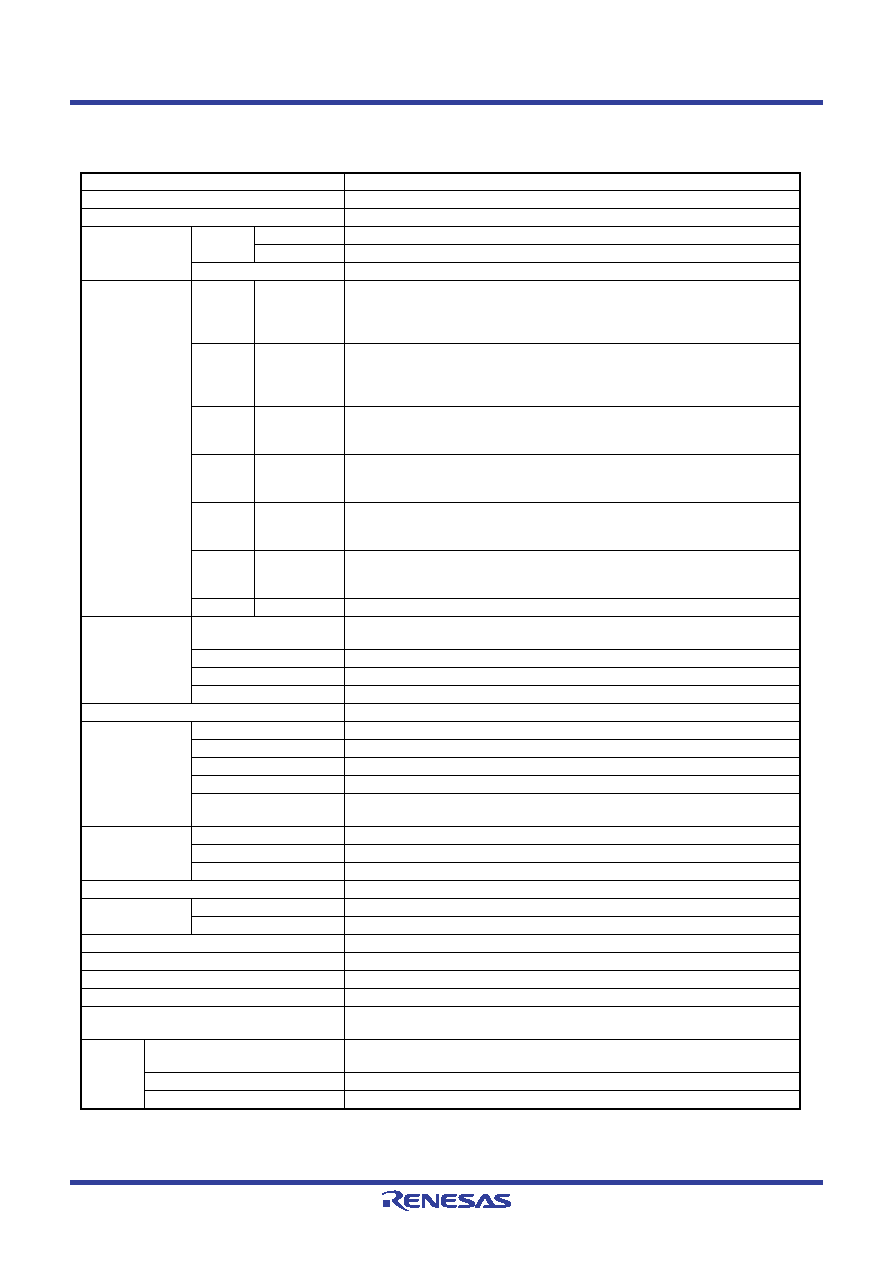
PERFORMANCE OVERVIEW
Table 2
Performance overview
Parameter
Function
Number of basic instructions
138
Minimum instruction execution time
0.5
s (Oscillation frequency 6 MHz: high-speed through mode)
Memory sizes
ROM
M3455AG8
8192 words
× 10 bits
M3455AGC
12288 words
× 10 bits
RAM
512 words
× 4 bits (including LCD display RAM 32 words × 4 bits)
I/O port
D0
D5
I/O
(Input is
examined by
skip decision.)
Six independent I/O ports. A pull-up function, a key-on wakeup function and output
structure can be switched by software.
Port D5 is also used as INT pin.
D6
, D7
I/O
(Input is
examined by
skip decision.)
Two independent I/O ports; each pin is equipped with a pull-up function and a key-on
wakeup function. Both functions can be switched by software.
Ports D6 and D7 are also used as XCIN and XCOUT, respectively.
P00
P03
I/O
4-bit I/O port; A pull-up function, a key-on wakeup function and output structure can
be switched by software.
Ports P00
P03 are also used as SEG16SEG19, respectively.
P10
P13
I/O
4-bit I/O port; A pull-up function, a key-on wakeup function and output structure can
be switched by software.
Ports P10
P13 are also used as SEG20SEG23, respectively.
P20
P23
I/O
4-bit I/O port; A pull-up function, a key-on wakeup function and output structure can
be switched by software.
Ports P20
P23 are also used as SEG24SEG27, respectively.
P30
P33
I/O
4-bit I/O port; A pull-up function, a key-on wakeup function and output structure can
be switched by software.
Ports P30
P33 are also used as SEG28SEG31, respectively.
C
Output
1-bit output; Port C is also used as CNTR pin.
Timer
Timer 1
8-bit timer with a reload register and carrier wave output auto-control function, and
has an event counter.
Timer 2
8-bit timer with two reload registers and carrier wave generation function.
Timer 3
16-bit timer, fixed dividing frequency (timer for clock count)
Timer LC
4-bit programmable timer with a reload register (for LCD clock generating)
Watchdog timer
16-bit timer, fixed dividing frequency (timer for monitor)
LCD control circuit
Selective bias value
1/2, 1/3 bias
Selective duty value
2, 3, 4 duty
Common output
4
Segment output
32
Internal resistor for power
supply
2r
× 3, 2r × 2, r × 3, r × 2 (r = 100 k, (Ta = 25 °C, Typical value))
Voltage drop
detection circuit
Reset occurrence
Typ. 1.7 V (Ta=25 °C)
Reset release
Typ. 1.8 V (Ta=25 °C)
Skip occurrence
Typ. 2.0 V (Ta=25 °C)
Power-on reset circuit
Built-in
Interrupt
Source
4 sources (one for external, three for timers)
Nesting
1 level
Subroutine nesting
8 levels
Device structure
CMOS silicon gate
Package
52-pin plastic molded LQFP (PLQP0052JA-A)
Operating temperature range
-20 to 85 °C
Power source voltage
1.8 to 5.5 V (It depends on operation source clock, oscillation frequency and
operation mode)
Power
dissipation
(Typ. value)
At active mode
0.3 mA (Ta = 25 °C, VDD
= 3.0 V, f(XIN) = 4 MHz, f(XCIN) = stop, f(HSOCO) = stop,
f(LSOCO)=stop, f(STCK) = f(XIN/8)
At clock operating mode
5
A (Ta = 25 °C, VDD = 3.0 V, f(XCIN) = 32 kHz)
At RAM back-up
0.1
A (Ta = 25 °C, output transistor is cut-off state)
相關(guān)PDF資料 |
PDF描述 |
|---|---|
| M34570MD-XXXFP | 4-BIT, MROM, 2 MHz, MICROCONTROLLER, PDSO36 |
| M34570E8FP | 4-BIT, OTPROM, 2 MHz, MICROCONTROLLER, PDSO36 |
| M34583EDFP | 4-BIT, OTPROM, 6 MHz, MICROCONTROLLER, PQFP32 |
| M34583MD-XXXFP | 4-BIT, MROM, 6 MHz, MICROCONTROLLER, PQFP32 |
| M34583MD-XXXFP | 4-BIT, MROM, 6 MHz, MICROCONTROLLER, PQFP32 |
相關(guān)代理商/技術(shù)參數(shù) |
參數(shù)描述 |
|---|---|
| M3455AGCFP | 制造商:RENESAS 制造商全稱:Renesas Technology Corp 功能描述:SINGLE-CHIP 4-BIT CMOS MICROCOMPUTER |
| M3455AGC-XXXFP | 制造商:RENESAS 制造商全稱:Renesas Technology Corp 功能描述:SINGLE-CHIP 4-BIT CMOS MICROCOMPUTER |
| M3455-SL001 | 制造商:Alpha Wire 功能描述: |
| M3455-SL002 | 制造商:Alpha Wire 功能描述: |
| M3455-SL005 | 制造商:Alpha Wire 功能描述: |
發(fā)布緊急采購(gòu),3分鐘左右您將得到回復(fù)。