- 您現(xiàn)在的位置:買賣IC網(wǎng) > PDF目錄45027 > M34286G2-XXXGP 4-BIT, MROM, 4 MHz, MICROCONTROLLER, PDSO20 PDF資料下載
參數(shù)資料
| 型號(hào): | M34286G2-XXXGP |
| 元件分類: | 微控制器/微處理器 |
| 英文描述: | 4-BIT, MROM, 4 MHz, MICROCONTROLLER, PDSO20 |
| 封裝: | 4.40 X 6.50 MM, 0.65 MM PITCH, PLASTIC, LSSOP-20 |
| 文件頁數(shù): | 13/30頁 |
| 文件大小: | 516K |
| 代理商: | M34286G2-XXXGP |
第1頁第2頁第3頁第4頁第5頁第6頁第7頁第8頁第9頁第10頁第11頁第12頁當(dāng)前第13頁第14頁第15頁第16頁第17頁第18頁第19頁第20頁第21頁第22頁第23頁第24頁第25頁第26頁第27頁第28頁第29頁第30頁
Rev.1.00
Aug 06, 2008
page 18 of 64
REJ03B0251-0100
4286 Group
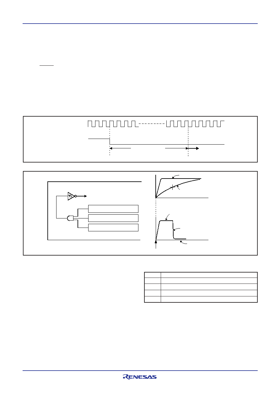
Fig. 19 Reset release timing
RESET FUNCTION
The 4286 Group has the power-on reset circuit, though it does
not have RESET pin. System reset is performed automatically
at power-on, and software starts program from address 0 in page
0.
In order to make the built-in power-on reset circuit operate
efficiently, set the voltage rising time until VDD= 0 to 2.2 V is
obtained at power-on 1ms or less (Ta = –20 °C to 85 °C).
Fig. 20 Power-on reset operation
f(XIN)
Internal reset signal
f(XIN) 16384 pulses
Software operation starts
(address 0 in page 0)
“H”
“L”
VDD
Internal reset signal
Power-on reset circuit
Voltage drop detection circuit
Watchdog timer output
Power-on reset circuit
output voltage
Reset state
Internal reset signal
Reset released
Power-on
Note on Power-on reset
Under the following condition, the system reset occurs by the
built-in the power-on reset circuit of this product;
-
when the supply voltage (VDD) rises from 0 V to 2.2 V, within
1 ms (Ta = –20 °C to 85 °C).
Also, note that system reset does not occur under the
following conditions;
-
when the supply voltage (VDD) rises from the voltage higher
than 0V, or
-
when it takes more than 1 ms for the supply voltage (VDD)
to rise from 0 V to 2.2 V (Ta = –20 °C to 85 °C).
(1) Internal state at reset
Table 6 shows port state at reset, and Figure 21 shows internal
state at reset (they are retained after system is released from
reset).
The contents of timers, registers, flags and RAM except shown
in Figure 21 are undefined, so set the initial value to them.
Table 6 Port state at reset
Name
D0–D7
G0–G3
E0, E1
CARR
State at reset
High impedance state (Pull-down transistor OFF)
“L” output
Note: The contents of all output latch is initialized to “0.”
相關(guān)PDF資料 |
PDF描述 |
|---|---|
| M34286G2GP | 4-BIT, MROM, 4 MHz, MICROCONTROLLER, PDSO20 |
| M34502M4-XXXFP | 4-BIT, MROM, 4.4 MHz, MICROCONTROLLER, PDSO24 |
| M34502M2-XXXFP | 4-BIT, MROM, 4.4 MHz, MICROCONTROLLER, PDSO24 |
| M34506M4-XXXFP | 4-BIT, MROM, MICROCONTROLLER, PDSO20 |
| M34506M2-XXXFP | 4-BIT, MROM, MICROCONTROLLER, PDSO20 |
相關(guān)代理商/技術(shù)參數(shù) |
參數(shù)描述 |
|---|---|
| M3429 SL001 | 制造商:Alpha Wire Company 功能描述:CBL 15PR 24AWG SLT 1000' |
| M3429 SL002 | 制造商:Alpha Wire Company 功能描述:CBL 15PR 24AWG SLT 500' |
| M3429 SL005 | 制造商:Alpha Wire Company 功能描述:CBL 15PR 24AWG SLT 100' |
| M34-2L | 制造商:BOWIN 制造商全稱:BOWIN 功能描述:SINGLE OUTPUT LED FLASHER IC |
| M342-SERIES | 制造商:未知廠家 制造商全稱:未知廠家 功能描述:Peripheral IC |
發(fā)布緊急采購,3分鐘左右您將得到回復(fù)。