- 您現(xiàn)在的位置:買賣IC網(wǎng) > PDF目錄370838 > M34282E2GP (Mitsubishi Electric Corporation) IC,CLK BUFFER,160MHZ,4 OUTPUT PDF資料下載
參數(shù)資料
第1頁第2頁第3頁第4頁第5頁第6頁第7頁第8頁第9頁第10頁第11頁第12頁第13頁第14頁第15頁第16頁第17頁第18頁第19頁第20頁第21頁第22頁第23頁第24頁第25頁第26頁第27頁第28頁第29頁第30頁第31頁第32頁第33頁第34頁第35頁第36頁第37頁第38頁第39頁第40頁第41頁第42頁第43頁第44頁第45頁第46頁第47頁第48頁第49頁第50頁第51頁第52頁第53頁第54頁第55頁第56頁第57頁第58頁第59頁第60頁第61頁第62頁當(dāng)前第63頁第64頁第65頁第66頁第67頁第68頁第69頁第70頁
MITSUBISHI
ELECTRIC
PRELIMINARY
Notice: This is not a final specification.
Some parametric limits are subject to change.
63
MITSUBISHI MICROCOMPUTERS
4282 Group
SINGLE-CHIP 4-BIT CMOS MICROCOMPUTER
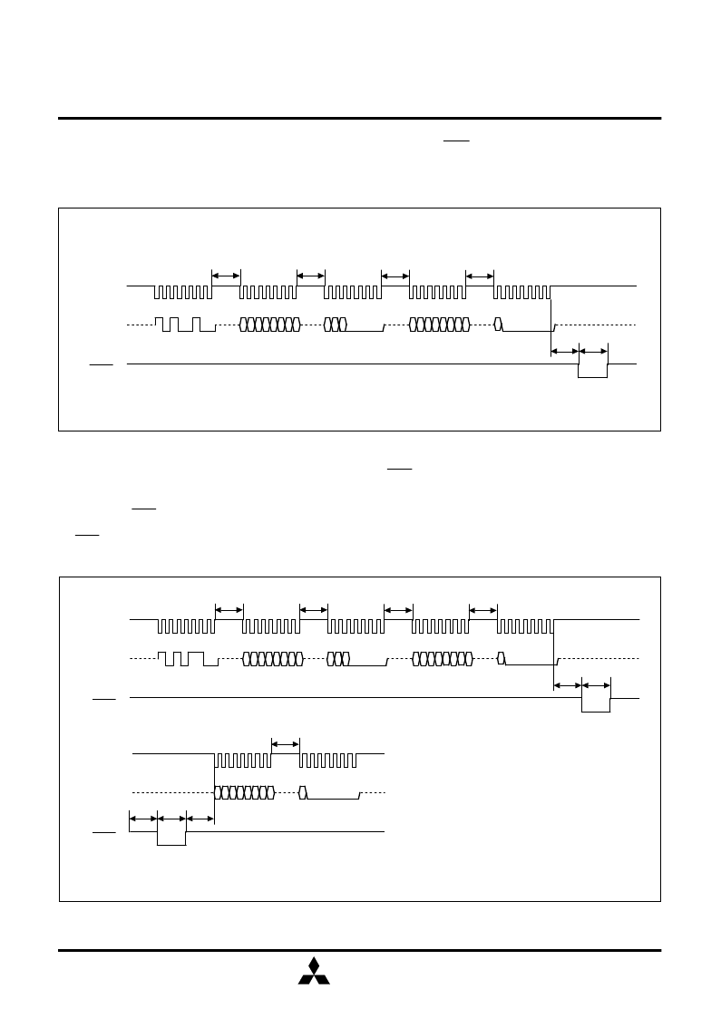
Fig. 31 Timing at program verifying
and pull the PGM pin to
“
L.
”
When this is done, the program
data is programmed to the specified address.
(4) Program
Input command code 25
16
in the first transfer. Proceed and
input the low-order 8 bits and high-order 8 bits of the address
and the low-order 8 bits and high-order 8 bits of program data,
Fig. 30 Timing at programming
(5) Program verify
Input command code 35
16
in the first transfer. Proceed and
input the low-order 8 bits and high-order 8 bits of the address
and the low-order 8 bits and high-order 8 bits of program data,
and pull the PGM pin to
“
L.
”
When this is done, the program
data is programmed to the specified address. Then, when the
PGM pin is pulled to
“
L
”
again after it is released back to
“
H,
”
the address programmed with the program command is read
and verified and stored into the internal data latch. When the
PGM pin is released back to
“
H
”
and serial clock is input to the
SCLK pin, the verify data that has been stored into the data
latch is serially output from the SDA pin.
Note: When outputting the verify data, the SDA pin is switched for output at the first falling of the serial clock. The SDA pin is
placed in the high-impedance state during the th
(C
–
E)
period after the last rising edge of the serial clock (at the 16th bit).
1 0 1 0 0 1 0 0
Commanf code input (25
16
)Program address input (L) Program address input (H)
A0
A7
SCLK
SDA
PGM
Program
t
CH
D0
D7
Program data input (L)
t
CP
t
WP
t
CH
D8
Program data input (H)
t
CH
0 0 0 0 0 0 0
t
CH
A8A9
0 0 0 0 0
A10
1 0 1 0 1 1 0 0
A0
A7
Command code input (35
16
)
Program address input (L)
Program address input (H)
SCLK
SDA
PGM
t
CH
D0
D7
Program data input (L)
t
CP
t
WP
t
CH
D8
Program data input (H)
t
CH
0 0 0 0 0 0 0
t
CH
A8A9
0 0 0 0 0
Program
t
CR
t
RC
SCLK
SDA
PGM
Verify
t
WR
D0
D7
Verify data output (L)
D8
Verify data output (H)
t
CH
0 0 0 0 0 0 0
A10
相關(guān)PDF資料 |
PDF描述 |
|---|---|
| M34501E4FP | SINGLE-CHIP 4-BIT CMOS MICROCOMPUTER |
| M34501M2 | SINGLE-CHIP 4-BIT CMOS MICROCOMPUTER |
| M34501M4 | SINGLE-CHIP 4-BIT CMOS MICROCOMPUTER |
| M34512M2 | SINGLE-CHIP 4-BIT CMOS MICROCOMPUTER |
| M34512M4 | SINGLE-CHIP 4-BIT CMOS MICROCOMPUTER |
相關(guān)代理商/技術(shù)參數(shù) |
參數(shù)描述 |
|---|---|
| M34282M1 | 制造商:MITSUBISHI 制造商全稱:Mitsubishi Electric Semiconductor 功能描述:SINGLE-CHIP 4-BIT CMOS MICROCOMPUTER |
| M34282M1-XXXGP | 制造商:MITSUBISHI 制造商全稱:Mitsubishi Electric Semiconductor 功能描述:SINGLE-CHIP 4-BIT CMOS MICROCOMPUTER |
| M34282M2 | 制造商:MITSUBISHI 制造商全稱:Mitsubishi Electric Semiconductor 功能描述:SINGLE-CHIP 4-BIT CMOS MICROCOMPUTER |
| M34282M2-064GP | 制造商:MITSUBISHI 制造商全稱:Mitsubishi Electric Semiconductor 功能描述:SINGLE-CHIP 4-BIT CMOS MICROCOMPUTER |
| M34282M2-XXXGP | 制造商:MITSUBISHI 制造商全稱:Mitsubishi Electric Semiconductor 功能描述:SINGLE-CHIP 4-BIT CMOS MICROCOMPUTER |
發(fā)布緊急采購,3分鐘左右您將得到回復(fù)。