- 您現(xiàn)在的位置:買賣IC網(wǎng) > PDF目錄296354 > M312L1713ETS-CAA 16M X 72 DDR DRAM MODULE, 0.75 ns, DMA184 PDF資料下載
參數(shù)資料
| 型號(hào): | M312L1713ETS-CAA |
| 元件分類: | DRAM |
| 英文描述: | 16M X 72 DDR DRAM MODULE, 0.75 ns, DMA184 |
| 封裝: | DIMM-184 |
| 文件頁(yè)數(shù): | 8/21頁(yè) |
| 文件大小: | 336K |
| 代理商: | M312L1713ETS-CAA |
第1頁(yè)第2頁(yè)第3頁(yè)第4頁(yè)第5頁(yè)第6頁(yè)第7頁(yè)當(dāng)前第8頁(yè)第9頁(yè)第10頁(yè)第11頁(yè)第12頁(yè)第13頁(yè)第14頁(yè)第15頁(yè)第16頁(yè)第17頁(yè)第18頁(yè)第19頁(yè)第20頁(yè)第21頁(yè)
DDR SDRAM
128MB, 256MB Registered DIMM
Rev. 1.2 August. 2003
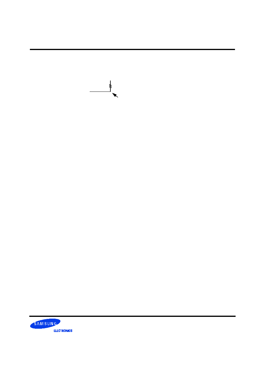
b. Pulldown slew rate is measured under the test conditions shown in Figure 2.
Output
Test point
VDDQ
50
Figure 2 : Pulldown slew rate test load
c. Pullup slew rate is measured between (VDDQ/2 - 320 mV +/- 250 mV)
Pulldown slew rate is measured between (VDDQ/2 + 320 mV +/- 250 mV)
Pullup and Pulldown slew rate conditions are to be met for any pattern of data, including all outputs switching and only one output
switching.
Example : For typical slew rate, DQ0 is switching
For minmum slew rate, all DQ bits are switching from either high to low, or low to high.
The remaining DQ bits remain the same as for previous state.
d. Evaluation conditions
Typical
: 25
°C (T Ambient), VDDQ = 2.5V, typical process
Minimum : 70
°C (T Ambient), VDDQ = 2.3V, slow - slow process
Maximum : 0
°C (T Ambient), VDDQ = 2.7V, fast - fast process
e. The ratio of pullup slew rate to pulldown slew rate is specified for the same temperature and voltage, over the entire temperature and
voltage range. For a given output, it represents the maximum difference between pullup and pulldown drivers due to process variation.
f. Verified under typical conditions for qualification purposes.
g. TSOPII package divices only.
h. Only intended for operation up to 266 Mbps per pin.
i. A derating factor will be used to increase tIS and tIH in the case where the input slew rate is below 0.5V/ns
as shown in Table 2. The Input slew rate is based on the lesser of the slew rates detemined by either VIH(AC) to VIL(AC) or
VIH(DC) to VIL(DC), similarly for rising transitions.
j. A derating factor will be used to increase tDS and tDH in the case where DQ, DM, and DQS slew rates differ, as shown in Tables 3 & 4.
Input slew rate is based on the larger of AC-AC delta rise, fall rate and DC-DC delta rise, Input slew rate is based on the lesser of the
slew rates determined by either VIH(AC) to VIL(AC) or VIH(DC) to VIL(DC), similarly for rising transitions.
The delta rise/fall rate is calculated as:
{1/(Slew Rate1)} - {1/(Slew Rate2)}
For example : If Slew Rate 1 is 0.5 V/ns and slew Rate 2 is 0.4 V/ns, then the delta rise, fall rate is - 0.5ns/V . Using the table given, this
would result in the need for an increase in tDS and tDH of 100 ps.
k. Table 3 is used to increase tDS and tDH in the case where the I/O slew rate is below 0.5 V/ns. The I/O slew rate is based on the lesser
on the lesser of the AC - AC slew rate and the DC- DC slew rate. The inut slew rate is based on the lesser of the slew rates deter
mined by either VIH(ac) to VIL(ac) or VIH(DC) to VIL(DC), and similarly for rising transitions.
m. DQS, DM, and DQ input slew rate is specified to prevent double clocking of data and preserve setup and hold times. Signal transi
tions through the DC region must be monotony.
相關(guān)PDF資料 |
PDF描述 |
|---|---|
| M312L5720BZ0-CB3 | 256M X 72 DDR DRAM MODULE, 0.7 ns, DMA184 |
| M312L5720DZ3-CB3 | 256M X 72 DDR DRAM MODULE, 0.7 ns, DMA184 |
| M32002AMMJFREQ | VCXO, CLOCK, 150 MHz - 1400 MHz, CMOS OUTPUT |
| M32016BGPJFREQ | VCXO, CLOCK, 150 MHz - 1400 MHz, PECL OUTPUT |
| M32026AUMJFREQ | VCXO, CLOCK, 150 MHz - 1400 MHz, CMOS OUTPUT |
相關(guān)代理商/技術(shù)參數(shù) |
參數(shù)描述 |
|---|---|
| M312L2828ET0 | 制造商:SAMSUNG 制造商全稱:Samsung semiconductor 功能描述:DDR SDRAM Registered Module |
| M312L2828ET0-CB000 | 制造商:Samsung Semiconductor 功能描述:512MDDRSTK_SMDDR SDRAM MODULX72TSOP2-400 - Bulk |
| M312L2920BG0 | 制造商:SAMSUNG 制造商全稱:Samsung semiconductor 功能描述:DDR SDRAM Registered Module |
| M312L2920BG0-A2 | 制造商:SAMSUNG 制造商全稱:Samsung semiconductor 功能描述:DDR SDRAM Registered Module |
| M312L2920BG0-B0 | 制造商:SAMSUNG 制造商全稱:Samsung semiconductor 功能描述:DDR SDRAM Registered Module |
發(fā)布緊急采購(gòu),3分鐘左右您將得到回復(fù)。