- 您現(xiàn)在的位置:買賣IC網(wǎng) > PDF目錄45019 > M30625MG-XXXGP 16-BIT, MROM, 16 MHz, MICROCONTROLLER, PQFP80 PDF資料下載
參數(shù)資料
| 型號: | M30625MG-XXXGP |
| 元件分類: | 微控制器/微處理器 |
| 英文描述: | 16-BIT, MROM, 16 MHz, MICROCONTROLLER, PQFP80 |
| 封裝: | PLASTIC, QFP-80 |
| 文件頁數(shù): | 11/230頁 |
| 文件大?。?/td> | 2870K |
| 代理商: | M30625MG-XXXGP |
第1頁第2頁第3頁第4頁第5頁第6頁第7頁第8頁第9頁第10頁當前第11頁第12頁第13頁第14頁第15頁第16頁第17頁第18頁第19頁第20頁第21頁第22頁第23頁第24頁第25頁第26頁第27頁第28頁第29頁第30頁第31頁第32頁第33頁第34頁第35頁第36頁第37頁第38頁第39頁第40頁第41頁第42頁第43頁第44頁第45頁第46頁第47頁第48頁第49頁第50頁第51頁第52頁第53頁第54頁第55頁第56頁第57頁第58頁第59頁第60頁第61頁第62頁第63頁第64頁第65頁第66頁第67頁第68頁第69頁第70頁第71頁第72頁第73頁第74頁第75頁第76頁第77頁第78頁第79頁第80頁第81頁第82頁第83頁第84頁第85頁第86頁第87頁第88頁第89頁第90頁第91頁第92頁第93頁第94頁第95頁第96頁第97頁第98頁第99頁第100頁第101頁第102頁第103頁第104頁第105頁第106頁第107頁第108頁第109頁第110頁第111頁第112頁第113頁第114頁第115頁第116頁第117頁第118頁第119頁第120頁第121頁第122頁第123頁第124頁第125頁第126頁第127頁第128頁第129頁第130頁第131頁第132頁第133頁第134頁第135頁第136頁第137頁第138頁第139頁第140頁第141頁第142頁第143頁第144頁第145頁第146頁第147頁第148頁第149頁第150頁第151頁第152頁第153頁第154頁第155頁第156頁第157頁第158頁第159頁第160頁第161頁第162頁第163頁第164頁第165頁第166頁第167頁第168頁第169頁第170頁第171頁第172頁第173頁第174頁第175頁第176頁第177頁第178頁第179頁第180頁第181頁第182頁第183頁第184頁第185頁第186頁第187頁第188頁第189頁第190頁第191頁第192頁第193頁第194頁第195頁第196頁第197頁第198頁第199頁第200頁第201頁第202頁第203頁第204頁第205頁第206頁第207頁第208頁第209頁第210頁第211頁第212頁第213頁第214頁第215頁第216頁第217頁第218頁第219頁第220頁第221頁第222頁第223頁第224頁第225頁第226頁第227頁第228頁第229頁第230頁
Clock asynchronous serial I/O (UART) mode
Mitsubishi microcomputers
M16C / 62 Group (80-pin)
SINGLE-CHIP 16-BIT CMOS MICROCOMPUTER
108
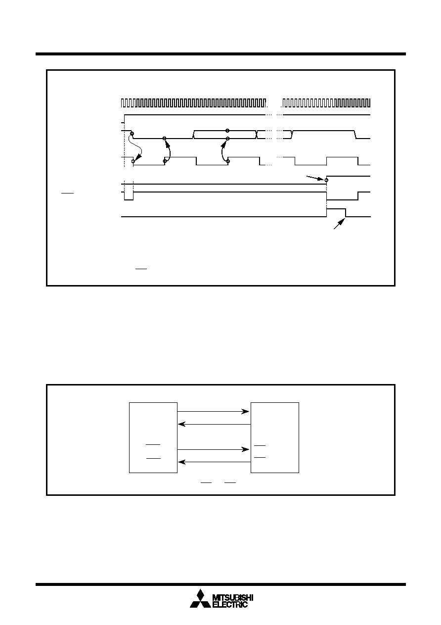
Example of receive timing when transfer data is 8 bits long (parity disabled, one stop bit)
Figure 1.14.18. Typical receive timing in UART mode
_______ _______
(a) Separate CTS/RTS pins function (UART0)
_______ _______
_______
Setting the CTS/RTS separate bit (bit 6 of address 03B016) to “1” inputs/outputs the CTS signal and
_______
_______ _______
RTS signal from different pins. Choose which to use, CTS or RTS, by use of the CTS/RTS function
select bit (bit 2 of address 03A416). This function is effective in UART0 only. With this function cho-
_______ _______
sen, the user cannot use the CTS/RTS function. Set "0" both to the CTS/RTS function select bit (bit
_______ _______
2 of address 03AC16) and to the CTS/RTS disable bit (bit 4 of address 03AC16).
This mode is used to transfer data between specific microcomputers among multiple microcomputers
connected using UARTi. The sleep mode is selected when the sleep select bit (bit 7 at addresses
03A016, 03A816) is set to “1” during reception. In this mode, the unit performs receive operation when
the MSB of the received data = “1” and does not perform receive operation when the MSB = “0”.
D0
Start bit
Sampled “L”
Receive data taken in
BRGi count
source
Receive enable bit
RxDi
Transfer clock
Receive
complete flag
RTSi
Stop bit
“1”
“0”
“1”
“H”
“L”
The above timing applies to the following settings :
Parity is disabled.
One stop bit.
RTS function is selected.
Receive interrupt
request bit
“0”
“1”
Transferred from UARTi receive register to
UARTi receive buffer register
Reception triggered when transfer clock
is generated by falling edge of start bit
D7
D1
Cleared to “0” when interrupt request is accepted, or cleared by software
Note: RTS in UART2 is not connected to the outside.
_______ _______
Figure 1.14.19. The separate CTS/RTS pins function usage
Microcomputer
TXD0 (P63)
RXD0 (P62)
IN
OUT
CTS
RTS
CTS0 (P64)
RTS0 (P60)
IC
Note : The user cannot use CTS and RTS at the same time.
相關PDF資料 |
PDF描述 |
|---|---|
| M30623MC-XXXGP | 16-BIT, MROM, 16 MHz, MICROCONTROLLER, PQFP80 |
| M30621MA-XXXGP | 16-BIT, MROM, 16 MHz, MICROCONTROLLER, PQFP80 |
| M30625FGGP | 16-BIT, FLASH, 16 MHz, MICROCONTROLLER, PQFP80 |
| M30625FGLGP | 16-BIT, FLASH, 16 MHz, MICROCONTROLLER, PQFP80 |
| M30625MG-XXXGP | 16-BIT, MROM, 16 MHz, MICROCONTROLLER, PQFP80 |
相關代理商/技術參數(shù) |
參數(shù)描述 |
|---|---|
| M30625MHP-XXXGP | 制造商:RENESAS 制造商全稱:Renesas Technology Corp 功能描述:SINGLE-CHIP 16-BIT CMOS MICROCOMPUTER |
| M30625MWP | 制造商:RENESAS 制造商全稱:Renesas Technology Corp 功能描述:SINGLE-CHIP 16-BIT CMOS MICROCOMPUTER |
| M30625MWP-XXXGP | 制造商:RENESAS 制造商全稱:Renesas Technology Corp 功能描述:SINGLE-CHIP 16-BIT CMOS MICROCOMPUTER |
| M30626FHPFP | 制造商:RENESAS 制造商全稱:Renesas Technology Corp 功能描述:SINGLE-CHIP 16-BIT CMOS MICROCOMPUTER |
| M30626FHPFP D5 | 制造商:Renesas Electronics Corporation 功能描述: |
發(fā)布緊急采購,3分鐘左右您將得到回復。