- 您現(xiàn)在的位置:買賣IC網(wǎng) > PDF目錄370836 > M30623MCA-B72GP (Mitsubishi Electric Corporation) SINGLE-CHIP 16-BIT CMOS MICROCOMPUTER PDF資料下載
參數(shù)資料
| 型號: | M30623MCA-B72GP |
| 廠商: | Mitsubishi Electric Corporation |
| 英文描述: | SINGLE-CHIP 16-BIT CMOS MICROCOMPUTER |
| 中文描述: | 單片16位CMOS微機 |
| 文件頁數(shù): | 16/184頁 |
| 文件大小: | 1734K |
| 代理商: | M30623MCA-B72GP |
第1頁第2頁第3頁第4頁第5頁第6頁第7頁第8頁第9頁第10頁第11頁第12頁第13頁第14頁第15頁當前第16頁第17頁第18頁第19頁第20頁第21頁第22頁第23頁第24頁第25頁第26頁第27頁第28頁第29頁第30頁第31頁第32頁第33頁第34頁第35頁第36頁第37頁第38頁第39頁第40頁第41頁第42頁第43頁第44頁第45頁第46頁第47頁第48頁第49頁第50頁第51頁第52頁第53頁第54頁第55頁第56頁第57頁第58頁第59頁第60頁第61頁第62頁第63頁第64頁第65頁第66頁第67頁第68頁第69頁第70頁第71頁第72頁第73頁第74頁第75頁第76頁第77頁第78頁第79頁第80頁第81頁第82頁第83頁第84頁第85頁第86頁第87頁第88頁第89頁第90頁第91頁第92頁第93頁第94頁第95頁第96頁第97頁第98頁第99頁第100頁第101頁第102頁第103頁第104頁第105頁第106頁第107頁第108頁第109頁第110頁第111頁第112頁第113頁第114頁第115頁第116頁第117頁第118頁第119頁第120頁第121頁第122頁第123頁第124頁第125頁第126頁第127頁第128頁第129頁第130頁第131頁第132頁第133頁第134頁第135頁第136頁第137頁第138頁第139頁第140頁第141頁第142頁第143頁第144頁第145頁第146頁第147頁第148頁第149頁第150頁第151頁第152頁第153頁第154頁第155頁第156頁第157頁第158頁第159頁第160頁第161頁第162頁第163頁第164頁第165頁第166頁第167頁第168頁第169頁第170頁第171頁第172頁第173頁第174頁第175頁第176頁第177頁第178頁第179頁第180頁第181頁第182頁第183頁第184頁
16
Mitsubishi microcomputers
M16C / 62T Group
SINGLE-CHIP 16-BIT CMOS MICROCOMPUTER
Reset
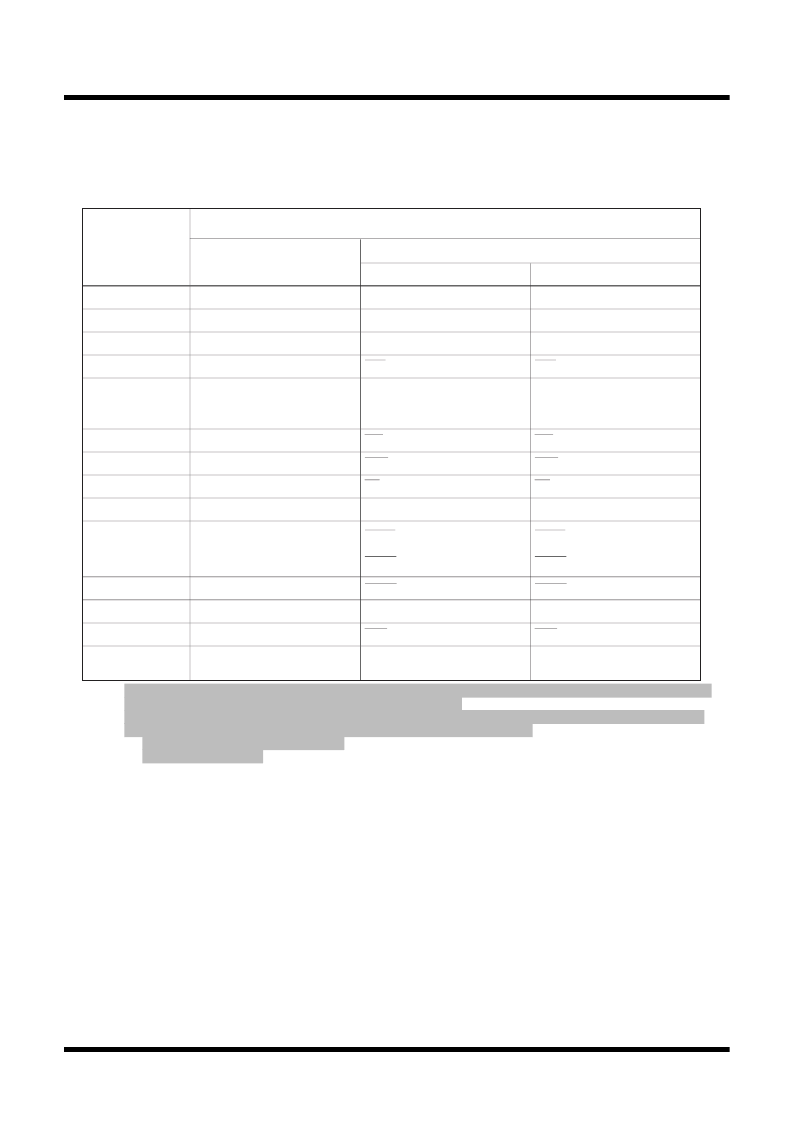
Table 1.6.1 shows the statuses of the other pins while the RESET pin level is “L”. Figures 1.6.3 and 1.6.4
show the internal status of the microcomputer immediately after the reset is cancelled.
Table 1.6.1. Pin status when RESET pin level is “L”
Status
CNV
SS
= V
CC
CNV
SS
= V
SS
BYTE = V
SS
(Note 1)
BYTE = V
CC
Pin
name
P0
P1
P2, P3, P4
0
to P4
3
P4
4
P4
5
to P4
7
P5
0
P5
1
P5
2
P5
3
P5
4
P5
5
P5
6
P5
7
P6, P7, P8
0
to P8
4
,
P8
6
, P8
7
, P9, P10
Note 1: In M30623(80-pin package), the BYTE signal has no external pin, and is internally connected to the CNV
SS
signal.
Accordingly, in the microprocessor mode, BYTE = CNV
SS
= V
CC
.
Note 2: In M30623(80-pin package), Port P1, P4
4
to P4
7
, P7
2
to P7
5
and P9
1
have no external pin, and are internally the
above conditions. After reset, set these ports to one of the following conditions.
Be output mode, and output “L” level.
Pull-up resister is on.
Input port (floating)
Input port (floating)
Input port (floating)
Input port (floating)
Input port (floating)
(pull-up resistor is on)
Input port (floating)
Input port (floating)
Input port (floating)
Input port (floating)
Input port (floating)
Input port (floating)
Input port (floating)
Input port (floating)
Input port (floating)
Data input (floating)
Data input (floating)
Address output (undefined)
BCLK output
ALE output (“L” level is output)
CS0 output (“H” level is output)
WR output (“H” level is output)
RD output (“H” level is output)
RDY input (floating)
Input port (floating)
BCLK output
BHE output (undefined)
HLDA output (The output value
depends on the input to the
HOLD pin)
HOLD input (floating)
Data input (floating)
Address output (undefined)
CS0 output (“H” level is output)
Input port (floating)
(pull-up resistor is on)
Input port (floating)
Input port (floating)
RDY input (floating)
ALE output (“L” level is output)
HOLD input (floating)
HLDA output (The output value
depends on the input to the
HOLD pin)
RD output (“H” level is output)
BHE output (undefined)
WR output (“H” level is output)
Input port (floating)
(pull-up resistor is on)
相關PDF資料 |
PDF描述 |
|---|---|
| M30623MAA-2MGP | SINGLE-CHIP 16-BIT CMOS MICROCOMPUTER |
| M30623M4A | SINGLE-CHIP 16-BIT CMOS MICROCOMPUTER |
| M30623M8A-2Y6GP | SINGLE-CHIP 16-BIT CMOS MICROCOMPUTER |
| M30625FGMGP | SINGLE-CHIP 16-BIT CMOS MICROCOMPUTER |
| M30625MGM-XXXGP | SINGLE-CHIP 16-BIT CMOS MICROCOMPUTER |
相關代理商/技術參數(shù) |
參數(shù)描述 |
|---|---|
| M30623MCA-XXXGP | 制造商:RENESAS 制造商全稱:Renesas Technology Corp 功能描述:SINGLE-CHIP 16-BIT CMOS MICROCOMPUTER |
| M30623MC-XXXGP | 制造商:RENESAS 制造商全稱:Renesas Technology Corp 功能描述:SINGLE-CHIP 16-BIT CMOS MICROCOMPUTER |
| M30623MEP | 制造商:RENESAS 制造商全稱:Renesas Technology Corp 功能描述:SINGLE-CHIP 16-BIT CMOS MICROCOMPUTER |
| M30623MEP-XXXGP | 制造商:RENESAS 制造商全稱:Renesas Technology Corp 功能描述:SINGLE-CHIP 16-BIT CMOS MICROCOMPUTER |
| M30623MG | 制造商:RENESAS 制造商全稱:Renesas Technology Corp 功能描述:SINGLE-CHIP 16-BIT CMOS MICROCOMPUTER |
發(fā)布緊急采購,3分鐘左右您將得到回復。