- 您現(xiàn)在的位置:買賣IC網(wǎng) > PDF目錄359727 > M30622MHP-XXXGP (Renesas Technology Corp.) SINGLE-CHIP 16-BIT CMOS MICROCOMPUTER PDF資料下載
參數(shù)資料
| 型號(hào): | M30622MHP-XXXGP |
| 廠商: | Renesas Technology Corp. |
| 英文描述: | SINGLE-CHIP 16-BIT CMOS MICROCOMPUTER |
| 中文描述: | 單片16位CMOS微機(jī) |
| 文件頁數(shù): | 19/87頁 |
| 文件大?。?/td> | 901K |
| 代理商: | M30622MHP-XXXGP |
第1頁第2頁第3頁第4頁第5頁第6頁第7頁第8頁第9頁第10頁第11頁第12頁第13頁第14頁第15頁第16頁第17頁第18頁當(dāng)前第19頁第20頁第21頁第22頁第23頁第24頁第25頁第26頁第27頁第28頁第29頁第30頁第31頁第32頁第33頁第34頁第35頁第36頁第37頁第38頁第39頁第40頁第41頁第42頁第43頁第44頁第45頁第46頁第47頁第48頁第49頁第50頁第51頁第52頁第53頁第54頁第55頁第56頁第57頁第58頁第59頁第60頁第61頁第62頁第63頁第64頁第65頁第66頁第67頁第68頁第69頁第70頁第71頁第72頁第73頁第74頁第75頁第76頁第77頁第78頁第79頁第80頁第81頁第82頁第83頁第84頁第85頁第86頁第87頁
M16C/62 Group (M16C/62P, M16C/62PT)
4
8
f
3
0
0
2
,
0
.
o
N
0
1
e
R
page 19
1. Overview
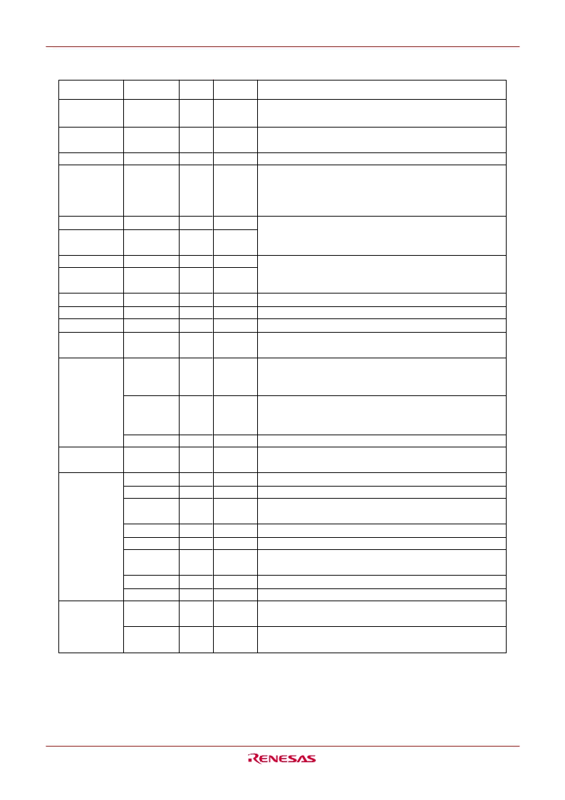
Apply 2.7 to 5.5 V to the VCC1 pin and 0 V to the VSS pin.
(2)
Applies the power supply for the A-D converter. Connect the AVCC pin to
VCC1. Connect the AVSS pin to VSS.
The microcomputer is in a reset state when applying "L" to the this pin.
Switches processor mode. Connect this pin to V
SS
to when after a reset to
start up in single-chip mode. Connect this pin to V
CC1
to start up in micropro-
cessor mode. As for the BYTE pin of the 80-pin versions, pull-up processing
is performed within the microcomputer.
I/O pins for the main clock generation circuit. Connect a ceramic resonator or
crystal oscillator between XIN and XOUT
(3)
. To use the external clock, input
the clock from XIN and leave XOUT open.
I/O pins for a sub clock oscillation circuit. Connect a crystal oscillator between
XCIN and XCOUT
(3)
. To use the external clock, input the clock from XCIN
and leave XCOUT open.
The clock of the same cycle as fC, f8, or f32 is outputted.
Input pins for the INT interrupt
Input pin for the NMI interrupt.
Input pins for the key input interrupt
These are timer A0, timer A3 and Timer A4 I/O pins. (except the output of
TAOUT for the N-channel open drain output.)
These are timer A0, timer A3 and Timer A4 input pins.
Input pin for the Z-phase.
These are timer B0, timer B2 to timer B5 input pins.
These are send control input pins.
These are receive control output pins.
These are transfer clock I/O pins.
These are serial data input pins.
These are serial data input pins.
These are serial data output pins. (except TXD2 for the N-channel open drain
output.)
These are serial data output pins.
This is output pin for transfer clock output from multiple pins function.
These are serial data I/O pins. (except SDA2 for the N-channel open drain
output.)
These are transfer clock I/O pins. (except SCL2 for the N-channel open drain
output.)
VCC1,
VSS
AVCC,
RESET
CNVSS
(BYTE)
XIN
XOUT
XCIN
XCOUT
_______
______
________
______
TA0OUT,
TA3OUT,
TA4OUT
TA0IN,
TA3IN,
TA4IN
ZP
TB0IN,
RTS0, RTS2
CLK0, CLK1,
CLK3, CLK4
RXD0 to RXD2
SIN4
TXD0 to TXD4
SOUT3, SOUT4
CLKS1
SDA0 to SDA2
SCL0 to SCL2
Power supply input
Analog power
supply input
Reset input
CNVSS
Main clock input
Main clock output
Sub clock input
Sub clock output
NMI interrupt input
Key input interrupt
input
Timer A
Timer B
Serial I/O
I
2
C mode
I
I
I
I
I
O
I
O
O
I
I
I
I/O
I
I
I
I
O
I/O
I
I
O
O
O
I/O
I/O
-
VCC1
VCC1
VCC1
VCC1
VCC1
VCC1
VCC1
VCC2
VCC1
VCC1
VCC1
VCC1
VCC1
VCC1
VCC1
VCC1
VCC1
VCC1
VCC1
VCC1
VCC1
VCC1
VCC1
VCC1
VCC1
Power
supply
Signal name Pin name
I/O type
Description
I : Input O : Output I/O : Input and output
NOTES:
1. In this manual, hereafter, VCC refers to VCC1 unless otherwise noted.
2. In M16C/62PT, apply 4.0 to 5.5 V to the VCC1 pin.
3. Ask the oscillator maker the oscillation characteristic.
Table 1.12 Pin Description (80-pin Version) (1)
相關(guān)PDF資料 |
PDF描述 |
|---|---|
| M30622MWP-XXXFP | SINGLE-CHIP 16-BIT CMOS MICROCOMPUTER |
| M30622MWP-XXXGP | SINGLE-CHIP 16-BIT CMOS MICROCOMPUTER |
| M30622SPFP | SINGLE-CHIP 16-BIT CMOS MICROCOMPUTER |
| M30622SPGP | SINGLE-CHIP 16-BIT CMOS MICROCOMPUTER |
| M30623F8PGP | SINGLE-CHIP 16-BIT CMOS MICROCOMPUTER |
相關(guān)代理商/技術(shù)參數(shù) |
參數(shù)描述 |
|---|---|
| M30622MWP | 制造商:RENESAS 制造商全稱:Renesas Technology Corp 功能描述:SINGLE-CHIP 16-BIT CMOS MICROCOMPUTER |
| M30622MWP-XXXFP | 制造商:RENESAS 制造商全稱:Renesas Technology Corp 功能描述:SINGLE-CHIP 16-BIT CMOS MICROCOMPUTER |
| M30622MWP-XXXGP | 制造商:RENESAS 制造商全稱:Renesas Technology Corp 功能描述:SINGLE-CHIP 16-BIT CMOS MICROCOMPUTER |
| M30622S4-XXXFP | 制造商:RENESAS 制造商全稱:Renesas Technology Corp 功能描述:16-BIT SINGLE-CHIP MICROCOMPUTER M16C FAMILY |
| M30622S4-XXXFS | 制造商:RENESAS 制造商全稱:Renesas Technology Corp 功能描述:16-BIT SINGLE-CHIP MICROCOMPUTER M16C FAMILY |
發(fā)布緊急采購,3分鐘左右您將得到回復(fù)。