- 您現(xiàn)在的位置:買賣IC網(wǎng) > PDF目錄370836 > M30622M8A-4C8FP (Mitsubishi Electric Corporation) SINGLE-CHIP 16-BIT CMOS MICROCOMPUTER PDF資料下載
第1頁第2頁第3頁第4頁第5頁第6頁第7頁第8頁第9頁第10頁第11頁第12頁第13頁第14頁第15頁第16頁第17頁第18頁第19頁第20頁第21頁第22頁第23頁第24頁第25頁第26頁第27頁第28頁第29頁第30頁第31頁第32頁第33頁第34頁第35頁第36頁第37頁第38頁第39頁第40頁第41頁第42頁第43頁第44頁第45頁第46頁第47頁第48頁第49頁第50頁第51頁第52頁第53頁第54頁第55頁第56頁第57頁第58頁第59頁第60頁第61頁第62頁第63頁第64頁第65頁第66頁第67頁第68頁第69頁第70頁第71頁第72頁第73頁第74頁第75頁第76頁第77頁第78頁第79頁第80頁第81頁第82頁第83頁第84頁第85頁第86頁第87頁第88頁第89頁第90頁第91頁第92頁第93頁第94頁第95頁第96頁第97頁第98頁第99頁第100頁第101頁第102頁第103頁第104頁第105頁第106頁第107頁第108頁第109頁第110頁第111頁第112頁第113頁第114頁第115頁第116頁第117頁第118頁第119頁第120頁第121頁第122頁第123頁第124頁第125頁第126頁第127頁第128頁第129頁第130頁第131頁第132頁第133頁第134頁第135頁第136頁第137頁第138頁第139頁第140頁第141頁第142頁第143頁第144頁第145頁第146頁第147頁第148頁第149頁第150頁第151頁第152頁第153頁第154頁第155頁第156頁第157頁第158頁第159頁第160頁第161頁第162頁第163頁第164頁第165頁第166頁第167頁第168頁第169頁第170頁第171頁第172頁第173頁第174頁第175頁第176頁第177頁第178頁第179頁第180頁第181頁第182頁第183頁第184頁第185頁第186頁第187頁第188頁第189頁第190頁第191頁第192頁第193頁第194頁第195頁第196頁第197頁第198頁第199頁第200頁第201頁第202頁第203頁第204頁第205頁第206頁第207頁第208頁第209頁第210頁第211頁第212頁第213頁第214頁第215頁第216頁第217頁第218頁第219頁第220頁第221頁第222頁第223頁第224頁第225頁第226頁第227頁第228頁第229頁第230頁第231頁第232頁第233頁第234頁第235頁第236頁第237頁第238頁第239頁第240頁第241頁第242頁第243頁第244頁第245頁第246頁第247頁第248頁第249頁第250頁第251頁第252頁第253頁第254頁第255頁第256頁第257頁當(dāng)前第258頁第259頁第260頁第261頁第262頁第263頁第264頁第265頁第266頁第267頁第268頁第269頁第270頁第271頁第272頁第273頁第274頁第275頁第276頁
Mitsubishi microcomputers
M16C / 62 Group
SINGLE-CHIP 16-BIT CMOS MICROCOMPUTER
Appendix Standard Serial I/O Mode (Flash Memory Version)
258
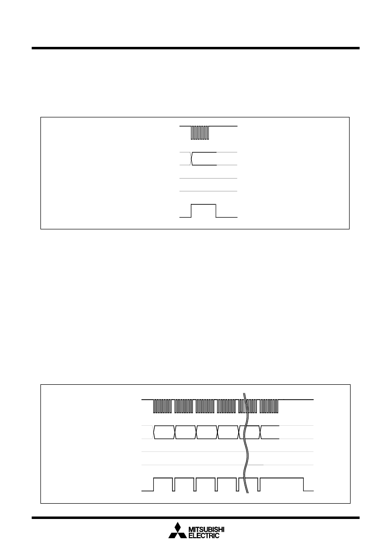
Figure 1.31.5. Timing for clearing the status register
Page Program Command
This command writes the specified page (256 bytes) in the flash memory sequentially one byte at a
time. Execute the page program command as explained here following.
(1) Send the
“
41
16
”
command code in the 1st byte of the transmission.
(2) Send addresses A
8
to A
15
and A
16
to A
23
in the 2nd and 3rd bytes of the transmission respectively.
(3) From the 4th byte onward, as write data (D
0
–
D
7
) for the page (256 bytes) specified with addresses
A
8
to A
23
is input sequentially from the smallest address first, that page is automatically written.
When reception setup for the next 256 bytes ends, the RTS1 (BUSY) signal changes from the
“
H
”
to
the
“
L
”
level. The result of the page program can be known by reading the status register. For more
information, see the section on the status register.
Each block can be write-protected with the lock bit. For more information, see the section on the data
protection function. Additional writing is not allowed with already programmed pages.
CLK1
RxD1
TxD1
RTS1(BUSY)
50
16
(M16C reception data)
(M16C transmit data)
Clear Status Register Command
This command clears the bits (SR3
–
SR5) which are set when the status register operation ends in
error. When the
“
50
16
”
command code is sent in the 1st byte of the transmission, the aforementioned
bits are cleared. When the clear status register operation ends, the RTS1 (BUSY) signal changes
from the
“
H
”
to the
“
L
”
level.
CLK1
RxD1
TxD1
RTS1(BUSY)
A
8
to
A
15
A
16
to
A
23
41
16
data0
data255
(M16C reception data)
(M16C transmit data)
Figure 1.31.6. Timing for the page program
相關(guān)PDF資料 |
PDF描述 |
|---|---|
| M30623M4T-246GP | SINGLE-CHIP 16-BIT CMOS MICROCOMPUTER |
| M30623ECVGP | SINGLE-CHIP 16-BIT CMOS MICROCOMPUTER |
| M30623MAH-A81GP | SINGLE-CHIP 16-BIT CMOS MICROCOMPUTER |
| M30623ECTGP | SINGLE-CHIP 16-BIT CMOS MICROCOMPUTER |
| M30623M4 | SINGLE-CHIP 16-BIT CMOS MICROCOMPUTER |
相關(guān)代理商/技術(shù)參數(shù) |
參數(shù)描述 |
|---|---|
| M30622M8A-8H0GP#U0 | 制造商:Renesas Electronics Corporation 功能描述: |
| M30622M8A-XXXFP | 制造商:MITSUBISHI 制造商全稱:Mitsubishi Electric Semiconductor 功能描述:SINGLE-CHIP 16-BIT CMOS MICROCOMPUTER |
| M30622M8A-XXXGP | 制造商:MITSUBISHI 制造商全稱:Mitsubishi Electric Semiconductor 功能描述:SINGLE-CHIP 16-BIT CMOS MICROCOMPUTER |
| M30622M8P- | 制造商:RENESAS 制造商全稱:Renesas Technology Corp 功能描述:SINGLE-CHIP 16-BIT CMOS MICROCOMPUTER |
| M30622M8P-XXXFP | 制造商:RENESAS 制造商全稱:Renesas Technology Corp 功能描述:SINGLE-CHIP 16-BIT CMOS MICROCOMPUTER |
發(fā)布緊急采購,3分鐘左右您將得到回復(fù)。