- 您現(xiàn)在的位置:買賣IC網(wǎng) > PDF目錄45015 > M30302GCPFP 16-BIT, OTPROM, 16 MHz, MICROCONTROLLER, PQFP100 PDF資料下載
參數(shù)資料
| 型號(hào): | M30302GCPFP |
| 元件分類: | 微控制器/微處理器 |
| 英文描述: | 16-BIT, OTPROM, 16 MHz, MICROCONTROLLER, PQFP100 |
| 封裝: | 14 X 20 MM, 0.65 MM PITCH, LEAD FREE, PLASTIC, LQFP-100 |
| 文件頁(yè)數(shù): | 5/57頁(yè) |
| 文件大小: | 649K |
| 代理商: | M30302GCPFP |
第1頁(yè)第2頁(yè)第3頁(yè)第4頁(yè)當(dāng)前第5頁(yè)第6頁(yè)第7頁(yè)第8頁(yè)第9頁(yè)第10頁(yè)第11頁(yè)第12頁(yè)第13頁(yè)第14頁(yè)第15頁(yè)第16頁(yè)第17頁(yè)第18頁(yè)第19頁(yè)第20頁(yè)第21頁(yè)第22頁(yè)第23頁(yè)第24頁(yè)第25頁(yè)第26頁(yè)第27頁(yè)第28頁(yè)第29頁(yè)第30頁(yè)第31頁(yè)第32頁(yè)第33頁(yè)第34頁(yè)第35頁(yè)第36頁(yè)第37頁(yè)第38頁(yè)第39頁(yè)第40頁(yè)第41頁(yè)第42頁(yè)第43頁(yè)第44頁(yè)第45頁(yè)第46頁(yè)第47頁(yè)第48頁(yè)第49頁(yè)第50頁(yè)第51頁(yè)第52頁(yè)第53頁(yè)第54頁(yè)第55頁(yè)第56頁(yè)第57頁(yè)
1. Overview
Page 13 of 53
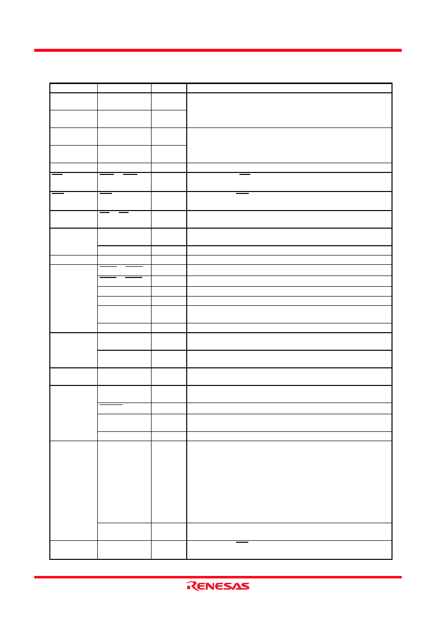
I : Input
O : Output
I/O : Input and output
Table 1.9
Pin Description (2)
Signal Name
Pin Name
I/O Type
Description
Main clock
input
XIN
I
I/O pins for the main clock generation circuit. Connect a ceramic
resonator or crystal oscillator between XIN and XOUT. To use the
external clock, input the clock from XIN and leave XOUT open.
Main clock
output
XOUT
O
Sub clock
input
XCIN
I
I/O pins for a sub clock oscillation circuit. Connect a crystal oscillator
between XCIN and XCOUT. To use the external clock, input the clock
from XCIN and leave XCOUT open.
Sub clock
output
XCOUT
O
Clock output
CLKOUT
O
The clock of the same cycle as fC, f8, or f32 is outputted.
INT interrupt
input
INT0 to INT4
I
Input pins for the INT interrupt.
NMI interrupt
input
NMI
I
Input pin for the NMI interrupt.
Key input
interrupt input
KI0 to KI3
I
Input pins for the key input interrupt.
Timer A
TA0OUT to
TA2OUT
I/O
These are timer A0 to timer A2 I/O pins. (however, the output of
TA0OUT for the N-channel open drain output.)
TA0IN to TA2IN
I
These are timer A0 to timer A2 input pins.
Timer B
TB0IN to TB2IN
I
These are timer B0 to timer B2 input pins.
Serial
interface
CTS0 to CTS2
I
These are send control input pins.
RTS0 to RTS2
O
These are receive control output pins.
CLK0 to CLK2
I/O
These are transfer clock I/O pins.
RXD0 to RXD2
I
These are serial data input pins.
TXD0 to TXD2
O
These are serial data output pins. (however, TXD2 for the N-channel
open drain output.)
CLKS1
O
This is output pin for transfer clock output from multiple pins function.
I2C mode
SDA0 to SDA2
I/O
These are serial data I/O pins. (however, SDA2 for the N-channel
open drain output.)
SCL0 to SCL2
I/O
These are transfer clock I/O pins. (however, SCL2 for the N-channel
open drain output.)
Reference
voltage input
VREF
I
Applies the reference voltage for the A/D converter.
A/D converter
AN0 to AN7,
AN0_0 to AN0_7
I
Analog input pins for the A/D converter.
ADTRG
I
This is an A/D trigger input pin.
ANEX0
I/O
This is the extended analog input pin for the A/D converter, and is the
output in external op-amp connection mode.
ANEX1
I
This is the extended analog input pin for the A/D converter.
I/O port
P0_0 to P0_7,
P1_0 to P1_7,
P2_0 to P2_7,
P3_0 to P3_7,
P4_0 to P4_7,
P5_0 to P5_7,
P6_0 to P6_7,
P7_0 to P7_7,
P9_0 to P9_7,
P10_0 to P10_7
I/O
8-bit I/O ports in CMOS, having a direction register to select an input
or output.
Each pin is set as an input port or output port. An input port can be set
for a pull-up or for no pull-up in 4-bit unit by program. (however, P7_0
and P7_1 for the N-channel open drain output.)
P8_0 to P8_4,
P8_6, P8_7
I/O
I/O ports having equivalent functions to P0.
Input port
P8_5
I
Input pin for the NMI interrupt. Pin states can be read by the P8_5 bit
in the P8 register.
相關(guān)PDF資料 |
PDF描述 |
|---|---|
| M30302GCPGP | 16-BIT, OTPROM, 16 MHz, MICROCONTROLLER, PQFP100 |
| M30304GEPGP | 16-BIT, OTPROM, 16 MHz, MICROCONTROLLER, PQFP100 |
| M30302MAP-XXXGP | 16-BIT, MROM, 16 MHz, MICROCONTROLLER, PQFP100 |
| M30302MEP-XXXGP | 16-BIT, MROM, 16 MHz, MICROCONTROLLER, PQFP100 |
| M30302GEPFP | 16-BIT, OTPROM, 16 MHz, MICROCONTROLLER, PQFP100 |
相關(guān)代理商/技術(shù)參數(shù) |
參數(shù)描述 |
|---|---|
| M30302GCPGP | 制造商:RENESAS 制造商全稱:Renesas Technology Corp 功能描述:SINGLE-CHIP 16-BIT CMOS MICROCOMPUTER |
| M30302GCP-XXXFP | 制造商:RENESAS 制造商全稱:Renesas Technology Corp 功能描述:SINGLE-CHIP 16-BIT CMOS MICROCOMPUTER |
| M30302GCP-XXXGP | 制造商:RENESAS 制造商全稱:Renesas Technology Corp 功能描述:SINGLE-CHIP 16-BIT CMOS MICROCOMPUTER |
| M30302GDPFP | 制造商:RENESAS 制造商全稱:Renesas Technology Corp 功能描述:SINGLE-CHIP 16-BIT CMOS MICROCOMPUTER |
| M30302GDPGP | 制造商:RENESAS 制造商全稱:Renesas Technology Corp 功能描述:SINGLE-CHIP 16-BIT CMOS MICROCOMPUTER |
發(fā)布緊急采購(gòu),3分鐘左右您將得到回復(fù)。