- 您現(xiàn)在的位置:買(mǎi)賣(mài)IC網(wǎng) > PDF目錄4414 > M1AGL1000V5-CS281I (Microsemi SoC)IC FPGA 1KB FLASH 1M 281-CSP PDF資料下載
參數(shù)資料
| 型號(hào): | M1AGL1000V5-CS281I |
| 廠商: | Microsemi SoC |
| 文件頁(yè)數(shù): | 194/250頁(yè) |
| 文件大?。?/td> | 0K |
| 描述: | IC FPGA 1KB FLASH 1M 281-CSP |
| 標(biāo)準(zhǔn)包裝: | 184 |
| 系列: | IGLOO |
| 邏輯元件/單元數(shù): | 24576 |
| RAM 位總計(jì): | 147456 |
| 輸入/輸出數(shù): | 215 |
| 門(mén)數(shù): | 1000000 |
| 電源電壓: | 1.425 V ~ 1.575 V |
| 安裝類(lèi)型: | 表面貼裝 |
| 工作溫度: | -40°C ~ 85°C |
| 封裝/外殼: | 281-TFBGA,CSBGA |
| 供應(yīng)商設(shè)備封裝: | 281-CSP(10x10) |
第1頁(yè)第2頁(yè)第3頁(yè)第4頁(yè)第5頁(yè)第6頁(yè)第7頁(yè)第8頁(yè)第9頁(yè)第10頁(yè)第11頁(yè)第12頁(yè)第13頁(yè)第14頁(yè)第15頁(yè)第16頁(yè)第17頁(yè)第18頁(yè)第19頁(yè)第20頁(yè)第21頁(yè)第22頁(yè)第23頁(yè)第24頁(yè)第25頁(yè)第26頁(yè)第27頁(yè)第28頁(yè)第29頁(yè)第30頁(yè)第31頁(yè)第32頁(yè)第33頁(yè)第34頁(yè)第35頁(yè)第36頁(yè)第37頁(yè)第38頁(yè)第39頁(yè)第40頁(yè)第41頁(yè)第42頁(yè)第43頁(yè)第44頁(yè)第45頁(yè)第46頁(yè)第47頁(yè)第48頁(yè)第49頁(yè)第50頁(yè)第51頁(yè)第52頁(yè)第53頁(yè)第54頁(yè)第55頁(yè)第56頁(yè)第57頁(yè)第58頁(yè)第59頁(yè)第60頁(yè)第61頁(yè)第62頁(yè)第63頁(yè)第64頁(yè)第65頁(yè)第66頁(yè)第67頁(yè)第68頁(yè)第69頁(yè)第70頁(yè)第71頁(yè)第72頁(yè)第73頁(yè)第74頁(yè)第75頁(yè)第76頁(yè)第77頁(yè)第78頁(yè)第79頁(yè)第80頁(yè)第81頁(yè)第82頁(yè)第83頁(yè)第84頁(yè)第85頁(yè)第86頁(yè)第87頁(yè)第88頁(yè)第89頁(yè)第90頁(yè)第91頁(yè)第92頁(yè)第93頁(yè)第94頁(yè)第95頁(yè)第96頁(yè)第97頁(yè)第98頁(yè)第99頁(yè)第100頁(yè)第101頁(yè)第102頁(yè)第103頁(yè)第104頁(yè)第105頁(yè)第106頁(yè)第107頁(yè)第108頁(yè)第109頁(yè)第110頁(yè)第111頁(yè)第112頁(yè)第113頁(yè)第114頁(yè)第115頁(yè)第116頁(yè)第117頁(yè)第118頁(yè)第119頁(yè)第120頁(yè)第121頁(yè)第122頁(yè)第123頁(yè)第124頁(yè)第125頁(yè)第126頁(yè)第127頁(yè)第128頁(yè)第129頁(yè)第130頁(yè)第131頁(yè)第132頁(yè)第133頁(yè)第134頁(yè)第135頁(yè)第136頁(yè)第137頁(yè)第138頁(yè)第139頁(yè)第140頁(yè)第141頁(yè)第142頁(yè)第143頁(yè)第144頁(yè)第145頁(yè)第146頁(yè)第147頁(yè)第148頁(yè)第149頁(yè)第150頁(yè)第151頁(yè)第152頁(yè)第153頁(yè)第154頁(yè)第155頁(yè)第156頁(yè)第157頁(yè)第158頁(yè)第159頁(yè)第160頁(yè)第161頁(yè)第162頁(yè)第163頁(yè)第164頁(yè)第165頁(yè)第166頁(yè)第167頁(yè)第168頁(yè)第169頁(yè)第170頁(yè)第171頁(yè)第172頁(yè)第173頁(yè)第174頁(yè)第175頁(yè)第176頁(yè)第177頁(yè)第178頁(yè)第179頁(yè)第180頁(yè)第181頁(yè)第182頁(yè)第183頁(yè)第184頁(yè)第185頁(yè)第186頁(yè)第187頁(yè)第188頁(yè)第189頁(yè)第190頁(yè)第191頁(yè)第192頁(yè)第193頁(yè)當(dāng)前第194頁(yè)第195頁(yè)第196頁(yè)第197頁(yè)第198頁(yè)第199頁(yè)第200頁(yè)第201頁(yè)第202頁(yè)第203頁(yè)第204頁(yè)第205頁(yè)第206頁(yè)第207頁(yè)第208頁(yè)第209頁(yè)第210頁(yè)第211頁(yè)第212頁(yè)第213頁(yè)第214頁(yè)第215頁(yè)第216頁(yè)第217頁(yè)第218頁(yè)第219頁(yè)第220頁(yè)第221頁(yè)第222頁(yè)第223頁(yè)第224頁(yè)第225頁(yè)第226頁(yè)第227頁(yè)第228頁(yè)第229頁(yè)第230頁(yè)第231頁(yè)第232頁(yè)第233頁(yè)第234頁(yè)第235頁(yè)第236頁(yè)第237頁(yè)第238頁(yè)第239頁(yè)第240頁(yè)第241頁(yè)第242頁(yè)第243頁(yè)第244頁(yè)第245頁(yè)第246頁(yè)第247頁(yè)第248頁(yè)第249頁(yè)第250頁(yè)
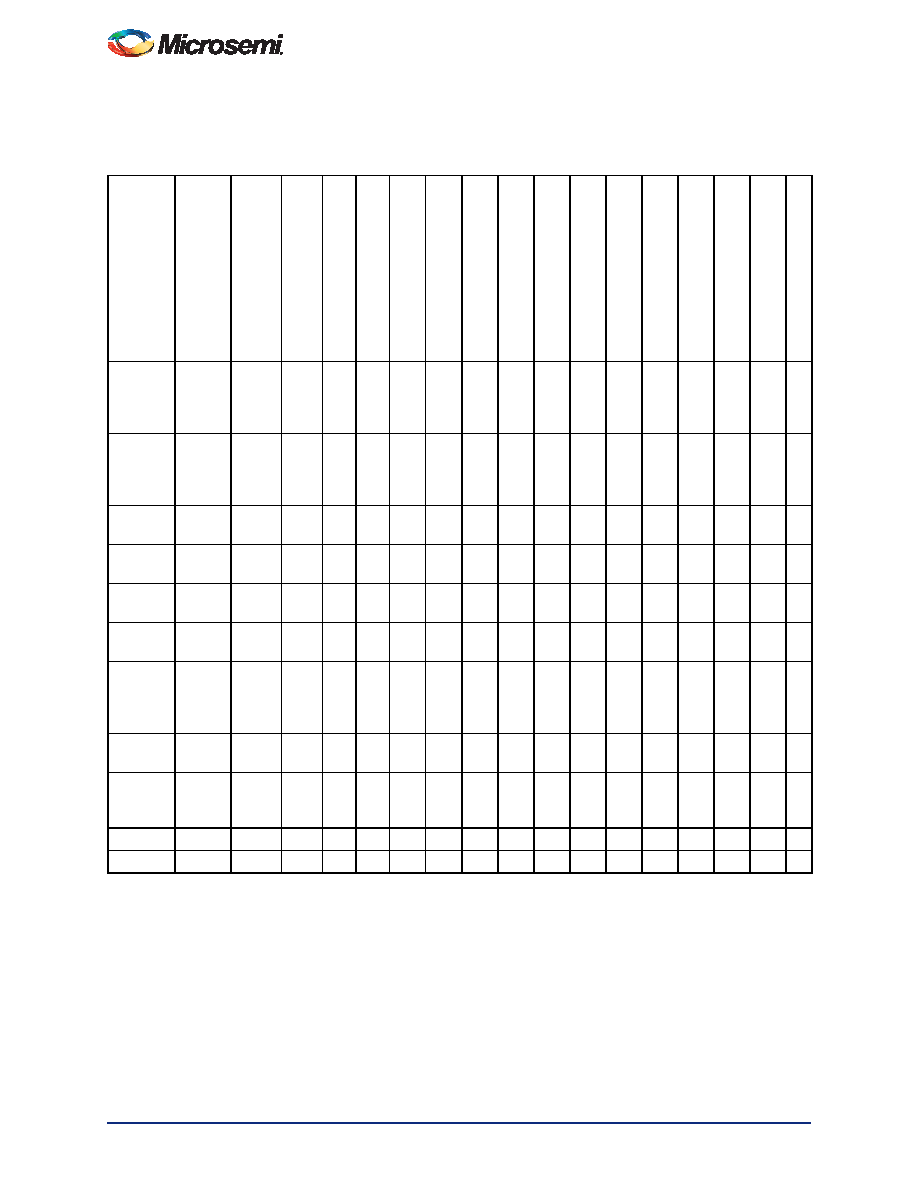
IGLOO DC and Switching Characteristics
2-32
Revision 23
Table 2-34 Summary of I/O Timing Characteristics—Software Default Settings, Std. Speed Grade,
Commercial-Case Conditions: TJ = 70°C, Worst-Case VCC = 1.14 V, Worst-Case VCCI (per
standard)
Applicable to Advanced I/O Banks
I/O
S
tan
dard
Dr
ive
S
trength
Eq
uivalen
tSo
ft
ware
Default
Drive
S
trength
Option
1
Slew
Rat
e
Ca
p
acitive
Lo
ad
(p
F)
Ex
te
rn
al
R
esi
st
or
(
)
t DO
UT
(ns)
t DP
(ns)
t DI
N
(ns)
t PY
(ns)
t EOUT
(ns)
t ZL
(ns)
t ZH
(ns)
t LZ
(ns)
t HZ
(ns)
t ZLS
(ns)
t ZH
S
(ns)
Unit
s
3.3 V
LVTTL /
3.3 V
LVCMOS
12 mA 12 mA High
5
–
1.55 2.67 0.26 0.98 1.10 2.71 2.18 3.25 3.93 8.50 7.97 ns
3.3 V
LVCMOS
Wide
Range2
100 A 12 mA High
5
–
1.55 3.73 0.26 1.32 1.10 3.73 2.91 4.51 5.43 9.52 8.69 ns
2.5 V
LVCMOS
12 mA 12 mA High
5
–
1.55 2.64 0.26 1.20 1.10 2.67 2.29 3.30 3.79 8.46 8.08 ns
1.8 V
LVCMOS
12 mA 12 mA High
5
–
1.55 2.72 0.26 1.11 1.10 2.76 2.43 3.58 4.19 8.55 8.22 ns
1.5 V
LVCMOS
12 mA 12 mA High
5
–
1.55 2.96 0.26 1.27 1.10 3.00 2.70 3.75 4.23 8.78 8.48 ns
1.2 V
LVCMOS
2 mA
High
5
–
1.55 3.60 0.26 1.60 1.10 3.47 3.36 3.93 3.65 9.26 9.14 ns
1.2 V
LVCMOS
Wide
Range3
100 A
2 mA
High
5
–
1.55 3.60 0.26 1.60 1.10 3.47 3.36 3.93 3.65 9.26 9.14 ns
3.3 V PCI Per PCI
spec
–
High
10 252 1.55 2.91 0.26 0.86 1.10 2.95 2.29 3.25 3.93 8.74 8.08 ns
3.3 V
PCI-X
Per
PCI-X
spec
–
High
10 252 1.55 2.91 0.25 0.86 1.10 2.95 2.29 3.25 3.93 8.74 8.08 ns
LVDS
24 mA
–
High
–
1.55 2.27 0.25 1.57
–
ns
LVPECL
24 mA
–
High
–
1.55 2.24 0.25 1.38
–
ns
Notes:
1. The minimum drive strength for any LVCMOS 1.2 V or LVCMOS 3.3 V software configuration when run in wide range is
±100 A. Drive strength displayed in the software is supported for normal range only. For a detailed I/V curve, refer to the
IBIS models.
2. All LVCMOS 3.3 V software macros support LVCMOS 3.3 V wide range as specified in the JESD-8B specification.
3. All LVCMOS 1.2 V software macros support LVCMOS 1.2 V wide range as specified in the JESD8-12 specification
4. Resistance is used to measure I/O propagation delays as defined in PCI specifications. See Figure 2-12 on page 2-78 for
connectivity. This resistor is not required during normal operation.
5. For specific junction temperature and voltage supply levels, refer to Table 2-6 on page 2-7 for derating values.
相關(guān)PDF資料 |
PDF描述 |
|---|---|
| RSA49DTMS | CONN EDGECARD 98POS R/A .125 SLD |
| EP4CGX50CF23C7 | IC CYCLONE IV GX FPGA 50K 484FBG |
| 24VL014T/MNY | IC EEPROM 1KBIT 400KHZ 8TDFN |
| A42MX24-1TQ176 | IC FPGA MX SGL CHIP 36K 176-TQFP |
| AT25160B-MAHL-T | IC EEPROM 16KBIT 20MHZ 8UDFN |
相關(guān)代理商/技術(shù)參數(shù) |
參數(shù)描述 |
|---|---|
| M1AGL1000V5-CSG144 | 制造商:ACTEL 制造商全稱:Actel Corporation 功能描述:IGLOO Low-Power Flash FPGAs with Flash Freeze Technology |
| M1AGL1000V5-CSG144ES | 制造商:ACTEL 制造商全稱:Actel Corporation 功能描述:IGLOO Low-Power Flash FPGAs with Flash Freeze Technology |
| M1AGL1000V5-CSG144I | 制造商:ACTEL 制造商全稱:Actel Corporation 功能描述:IGLOO Low-Power Flash FPGAs with Flash Freeze Technology |
| M1AGL1000V5-CSG144PP | 制造商:ACTEL 制造商全稱:Actel Corporation 功能描述:IGLOO Low-Power Flash FPGAs with Flash Freeze Technology |
| M1AGL1000V5-CSG281 | 功能描述:IC FPGA 1KB FLASH 1M 281-CSP RoHS:是 類(lèi)別:集成電路 (IC) >> 嵌入式 - FPGA(現(xiàn)場(chǎng)可編程門(mén)陣列) 系列:IGLOO 標(biāo)準(zhǔn)包裝:40 系列:SX-A LAB/CLB數(shù):6036 邏輯元件/單元數(shù):- RAM 位總計(jì):- 輸入/輸出數(shù):360 門(mén)數(shù):108000 電源電壓:2.25 V ~ 5.25 V 安裝類(lèi)型:表面貼裝 工作溫度:0°C ~ 70°C 封裝/外殼:484-BGA 供應(yīng)商設(shè)備封裝:484-FPBGA(27X27) |
發(fā)布緊急采購(gòu),3分鐘左右您將得到回復(fù)。