- 您現(xiàn)在的位置:買賣IC網(wǎng) > PDF目錄45008 > LX1673-09CPWTR (MICROSEMI CORP-ANALOG MIXED SIGNAL GROUP) 1 A SWITCHING CONTROLLER, 1035 kHz SWITCHING FREQ-MAX, PDSO20 PDF資料下載
參數(shù)資料
| 型號: | LX1673-09CPWTR |
| 廠商: | MICROSEMI CORP-ANALOG MIXED SIGNAL GROUP |
| 元件分類: | 穩(wěn)壓器 |
| 英文描述: | 1 A SWITCHING CONTROLLER, 1035 kHz SWITCHING FREQ-MAX, PDSO20 |
| 封裝: | PLASTIC, TSSOP-20 |
| 文件頁數(shù): | 6/13頁 |
| 文件大?。?/td> | 259K |
| 代理商: | LX1673-09CPWTR |
Microsemi
Linfinity Microelectronics Division
11861 Western Avenue, Garden Grove, CA. 92841, 714-898-8121, Fax: 714-893-2570
Page 2
Copyright
2000
Rev 0.4a, 5/25/2004
WWW
.Microse
m
i
.CO
M
LX1673
High Frequency PWM Regulator
PRELIMINARY DATA SHEET
TM
ABSOLUTE MAXIMUM RATINGS
Supply Voltage (VCC) DC................................................................-0.3V to 5.5V
Supply Voltage (VCC) Transient .........................................................-0.3V to 6V
Driver Supply Voltage (VCCL) DC .....................................................-0.3V to 13V
Driver Supply Voltage (VCCL) Transient............................................-0.3V to 16V
Driver Supply Voltage (VC1) DC .......................................................-0.3V to 19V
Input Voltage (SS/DIS) .....................................................................-0.3V to 5.5V
Output Drive Peak Current Source (HO, LO).......................................1A (500ns)
Output Drive Peak Current Sink (HO, LO) ..........................................1A (500ns)
Operating Temperature Range .........................................................-40
°C to 85°C
Maximum Operating Junction Temperature ................................................ 150
°C
Storage Temperature Range...........................................................-65
°C to 150°C
Lead Temperature (Soldering 180 seconds) ................................................ 235
°C
Package Peak Temp. for Solder Reflow (40 Seconds Maximum Exposure).. 255°C(+5, -0)
Note: Exceeding these ratings could cause damage to the device. All voltages are with respect to
Ground. Currents are positive into, negative out of specified terminal
.
The limitation on transient time is thermal and is due to zener diodes on the supply
pins, application of maximum voltages will increase current into that pin and
increase package power dissipation.
TH ERMAL DATA
PW
Plastic TSSOP 20-Pin
THERMAL RESISTANCE
-JUNCTION TO AMBIENT,
θ
JA
90
°C/W
LQ
Plastic MLPQ 20-Pin
THERMAL RESISTANCE
-JUNCTION TO AMBIENT,
θ
JA
35°C/W
Junction Temperature Calculation: TJ = TA + (PD x θJC).
The
θJA numbers are guidelines for the thermal performance of the device/pc-board system.
All of the above assume no airflow.
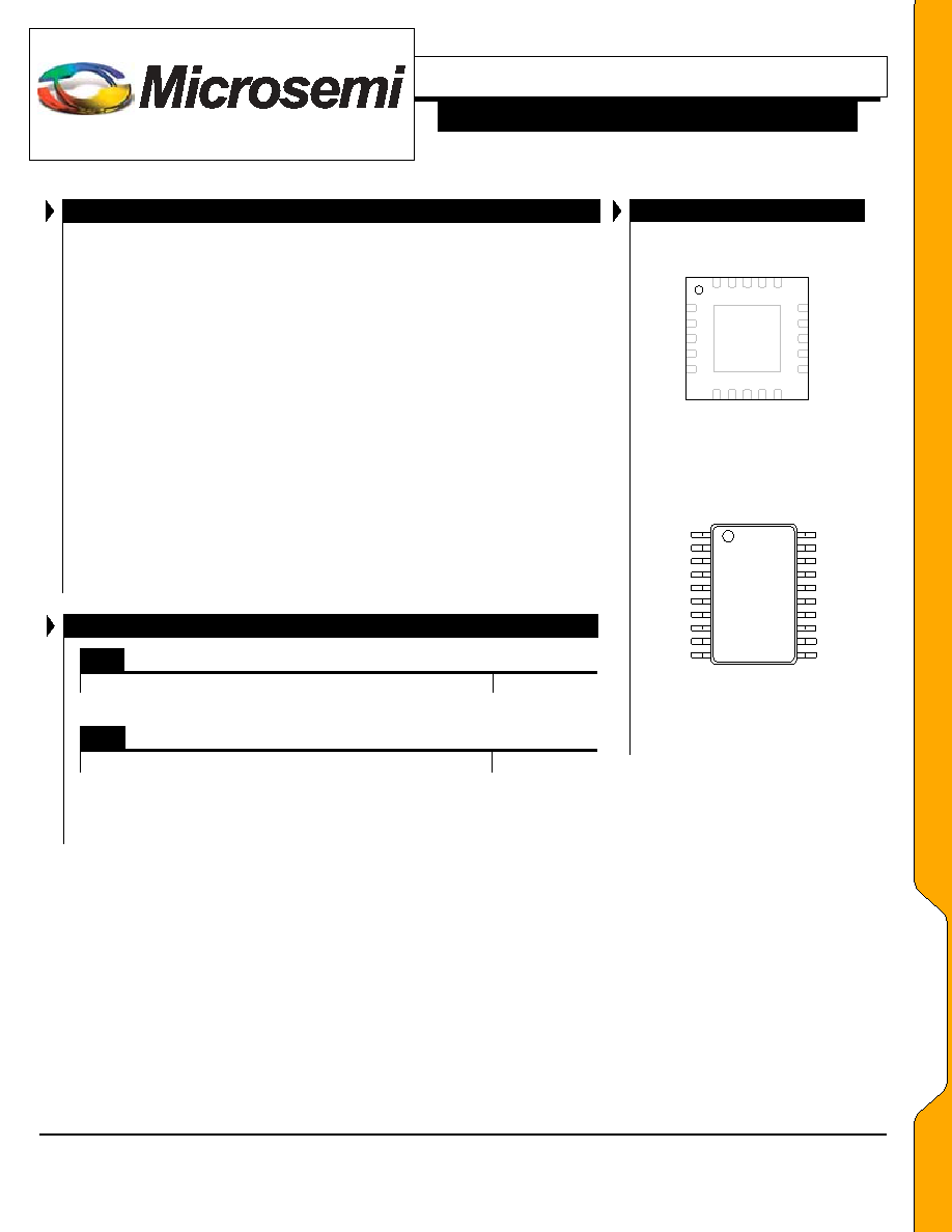
PACKAGE PIN OUT
LDGD
LDFB
LDDIS
DGND
AGND
CS
VS
VCC
VCCL
BDRV
PG
N
D
TD
R
V
VC
1
PW
G
D
LD
V
C
EAO
EA-
EA+
SS
DIS
1
6
11
16
LQ PACKAGE
(Top View)
N.C. – No Internal Connection
N/U – Not Used
RSVD – Do Not Use
VC1
PGOOD
LDOVCC
LDGD
LDFB
LDDIS
DGND
AGND
EAO
CS
VS
VCC
VCCL
BDRV
PGND
TDRV
1
10
11
20
DIS
SS
EA+
EA-
PW PACKAGE
(Top View)
Pb-free 100% Matte Tin Lead Finish
PP
AA
CC
KK
AA
GG
EE
DD
AA
TT
AA
相關(guān)PDF資料 |
PDF描述 |
|---|---|
| LX1673-06CLQ | 1 A SWITCHING CONTROLLER, 690 kHz SWITCHING FREQ-MAX, PQCC20 |
| LX1673-03CPW-TR | 1 A SWITCHING CONTROLLER, 345 kHz SWITCHING FREQ-MAX, PDSO20 |
| LX1673-03CPW | 1 A SWITCHING CONTROLLER, 345 kHz SWITCHING FREQ-MAX, PDSO20 |
| LX1673-03CLQ | 1 A SWITCHING CONTROLLER, 345 kHz SWITCHING FREQ-MAX, PQCC20 |
| LX1677CLQ-TR | 1.5 A SWITCHING CONTROLLER, 1100 kHz SWITCHING FREQ-MAX, PQCC38 |
相關(guān)代理商/技術(shù)參數(shù) |
參數(shù)描述 |
|---|---|
| LX1673-09CPW-TR | 制造商:Microsemi Corporation 功能描述:VOLT MODE PWM CNTRLR 0.8V TO 5.5V 1A 20TSSOP - Tape and Reel |
| LX1675 | 制造商:MICROSEMI 制造商全稱:Microsemi Corporation 功能描述:Multiple Output LoadSHARE⑩ PWM PRODUCTION DATA SHEET |
| LX1675 EVAL KIT | 制造商:Microsemi Corporation 功能描述:PWM CONTROLLERS - Bulk |
| LX1675CLQ | 制造商:Microsemi Corporation 功能描述: 制造商:Microsemi Corporation 功能描述:Voltage Mode PWM Controller 1.5A 38-Pin MLPQ |
| LX1675ILQ | 制造商:MICROSEMI 制造商全稱:Microsemi Corporation 功能描述:Multiple Output LoadSHARE⑩ PWM PRODUCTION DATA SHEET |
發(fā)布緊急采購,3分鐘左右您將得到回復(fù)。