- 您現(xiàn)在的位置:買賣IC網(wǎng) > PDF目錄9512 > LTC6990HS6#TRMPBF (Linear Technology)IC OSC SILICON 1MHZ TSOT23-6 PDF資料下載
參數(shù)資料
| 型號(hào): | LTC6990HS6#TRMPBF |
| 廠商: | Linear Technology |
| 文件頁數(shù): | 14/30頁 |
| 文件大?。?/td> | 0K |
| 描述: | IC OSC SILICON 1MHZ TSOT23-6 |
| 產(chǎn)品培訓(xùn)模塊: | TimerBlox Family Timing Devices |
| 產(chǎn)品目錄繪圖: | LTC699_TSOT-23 |
| 特色產(chǎn)品: | TimerBlox? |
| 標(biāo)準(zhǔn)包裝: | 1 |
| 系列: | TimerBlox® |
| 類型: | 振蕩器 - 硅 |
| 頻率: | 488Hz ~ 1MHz |
| 電源電壓: | 2.25 V ~ 5.5 V |
| 電流 - 電源: | 235µA |
| 工作溫度: | -40°C ~ 125°C |
| 封裝/外殼: | SOT-23-6 細(xì)型,TSOT-23-6 |
| 包裝: | 標(biāo)準(zhǔn)包裝 |
| 供應(yīng)商設(shè)備封裝: | TSOT-23-6 |
| 安裝類型: | 表面貼裝 |
| 配用: | DC1562A-A-ND - BOARD EVAL LTC6990 |
| 其它名稱: | LTC6990HS6#TRMPBFDKR |
第1頁第2頁第3頁第4頁第5頁第6頁第7頁第8頁第9頁第10頁第11頁第12頁第13頁當(dāng)前第14頁第15頁第16頁第17頁第18頁第19頁第20頁第21頁第22頁第23頁第24頁第25頁第26頁第27頁第28頁第29頁第30頁
LTC6990
21
6990fc
For more information www.linear.com/LTC6990
6990 F17
LTC6990
OE
GND
SET
OUT
V+
DIV
C1
0.1F
R1
R2
RSET
V+
DIV
SET
OUT
GND
OE
C1
R1
R2
V+
RSET
DCB PACKAGE
OE
GND
SET
OUT
V+
DIV
R2
V+
RSET
TSOT-23 PACKAGE
R1
C1
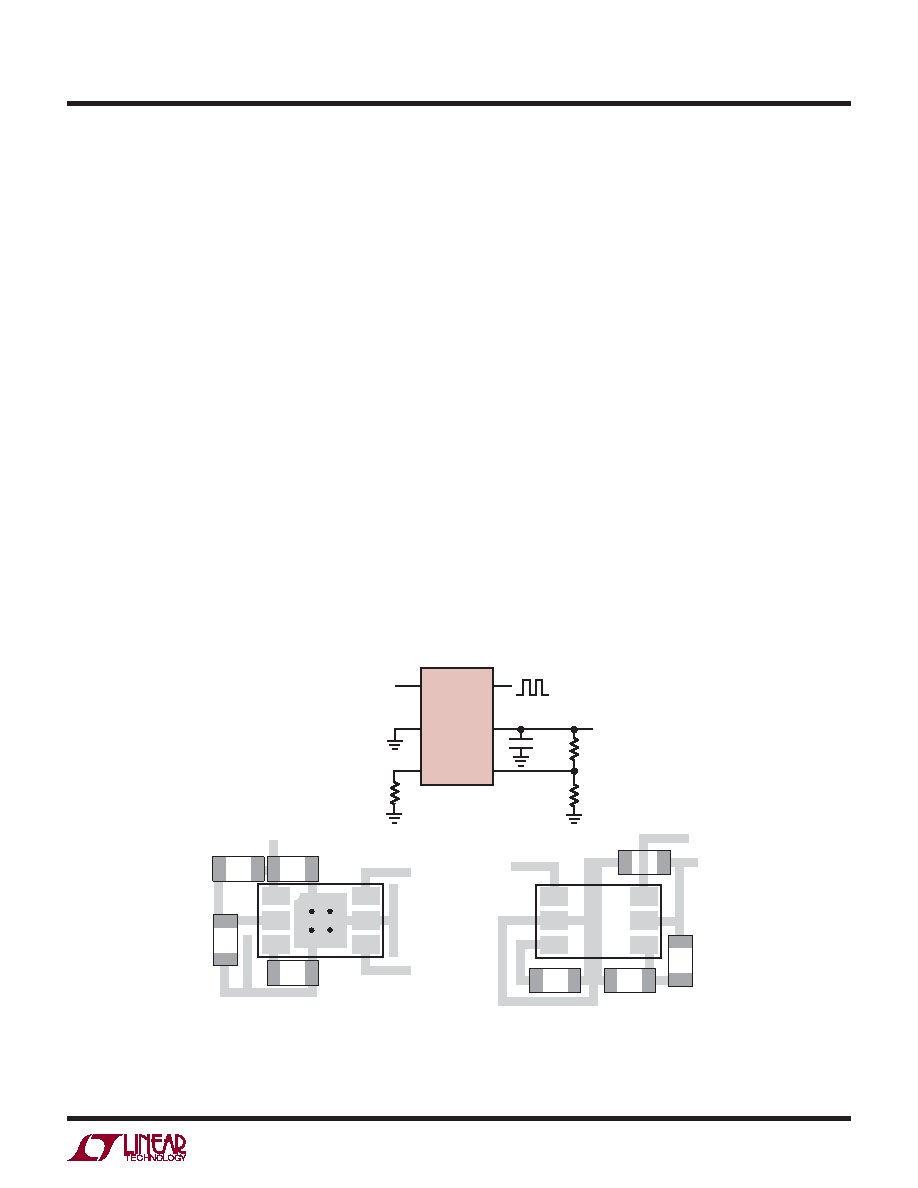
Figure 17. Supply Bypassing and PCB Layout
APPLICATIONS INFORMATION
SUPPLY BYPASSING AND PCB LAYOUT GUIDELINES
The LTC6990 is a 2.2% accurate silicon oscillator when
used in the appropriate manner. The part is simple to use
and by following a few rules, the expected performance
is easily achieved. The most important use issues involve
adequate supply bypassing and proper PCB layout.
Figure 17 shows example PCB layouts for both the SOT-23
and DCB packages using 0603 sized passive components.
The layouts assume a two layer board with a ground plane
layer beneath and around the LTC6990. These layouts are
a guide and need not be followed exactly.
1. Connect the bypass capacitor, C1, directly to the V+and
GND pins using a low inductance path. The connection
from C1 to the V+ pin is easily done directly on the top
layer. For the DCB package, C1’s connection to GND is
also simply done on the top layer. For the SOT-23, OUT
can be routed through the C1 pads to allow a good C1
GND connection. If the PCB design rules do not allow
that,C1’sGNDconnectioncanbeaccomplishedthrough
multiple vias to the ground plane. Multiple vias for both
the GND pin connection to the ground plane and the
C1 connection to the ground plane are recommended
to minimize the inductance. Capacitor C1 should be a
0.1F ceramic capacitor.
2. Place all passive components on the top side of the
board. This minimizes trace inductance.
3. Place RSET as close as possible to the SET pin and
make a direct, short connection. The SET pin is a
current summing node and currents injected into this
pin directly modulate the operating frequency. Having
a short connection minimizes the exposure to signal
pickup.
4. Connect RSET directly to the GND pin. Using a long path
or vias to the ground plane will not have a significant
affect on accuracy, but the direct, short connection is
recommended and easy to apply.
5. Use a ground trace to shield the SET pin. This provides
another layer of protection from radiated signals.
6. Place R1 and R2 close to the DIV pin. A direct, short
connection to the DIV pin minimizes the external signal
coupling.
相關(guān)PDF資料 |
PDF描述 |
|---|---|
| V110A8M200B2 | CONVERTER MOD DC/DC 8V 200W |
| V110A3V3M200BG3 | CONVERTER MOD DC/DC 3.3V 200W |
| V110A3V3M200BG2 | CONVERTER MOD DC/DC 3.3V 200W |
| M83723/85W803N | CONN RCPT 3POS JAM NUT W/PINS |
| V110A3V3M200BF3 | CONVERTER MOD DC/DC 3.3V 200W |
相關(guān)代理商/技術(shù)參數(shù) |
參數(shù)描述 |
|---|---|
| LTC6990HS6TRPBF | 制造商:LINER 制造商全稱:Linear Technology 功能描述:TimerBlox: Voltage Controlled Silicon Oscillator |
| LTC6990HS6-TRPBF | 制造商:LINER 制造商全稱:Linear Technology 功能描述:TimerBlox: Voltage Controlled Silicon Oscillator |
| LTC6990IDCB#PBF | 制造商:Linear Technology 功能描述: |
| LTC6990IDCB#TRMPBF | 功能描述:IC OSC SILICON 1MHZ 6DFN RoHS:是 類別:集成電路 (IC) >> 時(shí)鐘/計(jì)時(shí) - 可編程計(jì)時(shí)器和振蕩器 系列:TimerBlox® 產(chǎn)品培訓(xùn)模塊:Lead (SnPb) Finish for COTS Obsolescence Mitigation Program 標(biāo)準(zhǔn)包裝:45 系列:- 類型:溫度 - 補(bǔ)償晶體振蕩器(TCXO) 計(jì)數(shù):- 頻率:25MHz 電源電壓:3.135 V ~ 3.465 V 電流 - 電源:1.5mA 工作溫度:-40°C ~ 85°C 封裝/外殼:16-SOIC(0.295",7.50mm 寬) 包裝:管件 供應(yīng)商設(shè)備封裝:16-SOIC W 安裝類型:表面貼裝 |
| LTC6990IDCB#TRPBF | 功能描述:IC OSC SILICON 1MHZ 6DFN RoHS:是 類別:集成電路 (IC) >> 時(shí)鐘/計(jì)時(shí) - 可編程計(jì)時(shí)器和振蕩器 系列:TimerBlox® 產(chǎn)品培訓(xùn)模塊:Lead (SnPb) Finish for COTS Obsolescence Mitigation Program 標(biāo)準(zhǔn)包裝:45 系列:- 類型:溫度 - 補(bǔ)償晶體振蕩器(TCXO) 計(jì)數(shù):- 頻率:25MHz 電源電壓:3.135 V ~ 3.465 V 電流 - 電源:1.5mA 工作溫度:-40°C ~ 85°C 封裝/外殼:16-SOIC(0.295",7.50mm 寬) 包裝:管件 供應(yīng)商設(shè)備封裝:16-SOIC W 安裝類型:表面貼裝 |
發(fā)布緊急采購,3分鐘左右您將得到回復(fù)。