- 您現(xiàn)在的位置:買賣IC網(wǎng) > PDF目錄44995 > LTC3879EUD#TRPBF (LINEAR TECHNOLOGY CORP) SWITCHING CONTROLLER, PQCC16 PDF資料下載
參數(shù)資料
| 型號: | LTC3879EUD#TRPBF |
| 廠商: | LINEAR TECHNOLOGY CORP |
| 元件分類: | 穩(wěn)壓器 |
| 英文描述: | SWITCHING CONTROLLER, PQCC16 |
| 封裝: | 3 X 3 MM, LEAD FREE, PLASTIC, MO-220WEED-4, QFN-16 |
| 文件頁數(shù): | 4/28頁 |
| 文件大小: | 302K |
| 代理商: | LTC3879EUD#TRPBF |
第1頁第2頁第3頁當前第4頁第5頁第6頁第7頁第8頁第9頁第10頁第11頁第12頁第13頁第14頁第15頁第16頁第17頁第18頁第19頁第20頁第21頁第22頁第23頁第24頁第25頁第26頁第27頁第28頁
LTC3879
12
3879f
The resulting power dissipation in the MOSFETs at maxi-
mum output current are:
PD
I
R
V
TOP
OUT MAX
TOP
DS ON MAX
=
+
()
(
)
(
)()
2 ρτ
IIN
OUT MAX
MILLER
TGHIGH
INTVC
I
C
DR
V
2
()
()
C
MILLER
TGLOW
MILLER
OSC
BOT
BO
V
DR
V
f
PD
–
+
=
T
OUT MAX
BOT
DS ON MAX
IR
()
(
)
(
)()
2 ρτ
DRTGHIGH is pull-up driver resistance and DRTGLOW is the
TG driver pull-down resistance. VMILLER is the Miller ef-
fect VGS voltage and is taken graphically from the power
MOSFET data sheet.
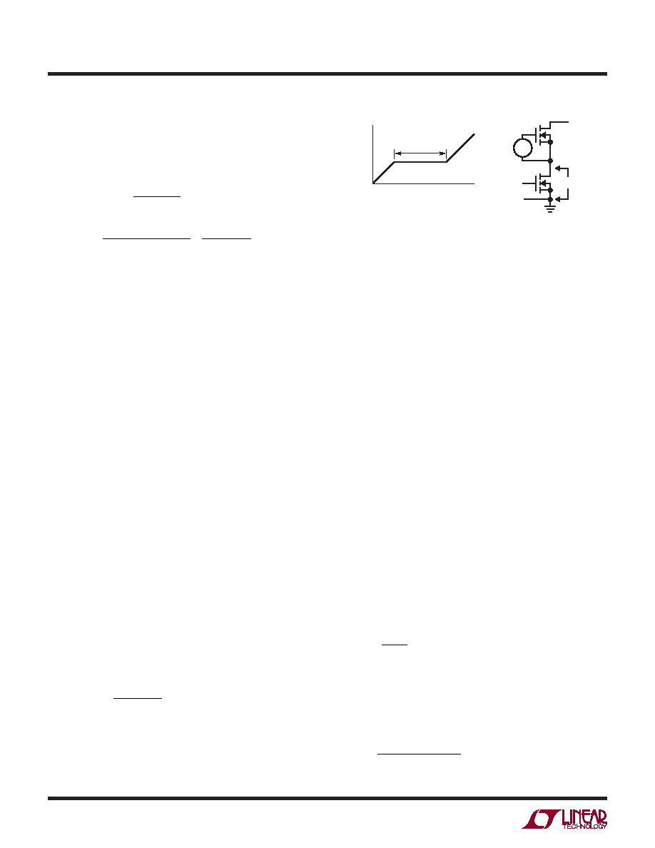
MOSFET input capacitance is a combination of several
components but can be taken from the typical “gate charge”
curve included on the most data sheets (Figure 2). The
curve is generated by forcing a constant input current
into the gate of a common source, current source, loaded
stage and then plotting the gate versus time. The initial
slope is the effect of the gate-to-source and gate-to-drain
capacitance. The at portion of the curve is the result of the
Miller multiplication effect of the drain-to-gate capacitance
as the drain drops the voltage across the current source
load. The upper sloping line is due to the drain-to-gate
accumulation capacitance and the gate-to-source capaci-
tance. The Miller charge (the increase in coulombs on the
horizontal axis from a to b while the curve is at) is speci-
ed from a given VDS drain voltage, but can be adjusted
for different VDS voltages by multiplying by the ratio of
the application VDS to the curve specied VDS values. A
way to estimate the CMILLER term is to take the change in
gate charge from points a and b or the parameter QGD on
a manufacturers data sheet and divide by the specied
VDS test voltage, VDS(TEST).
C
Q
V
MILLER
GD
DS TEST
=
()
CMILLER is the most important selection criteria for deter-
mining the transition loss term in the top MOSFET but is
not directly specied on MOSFET data sheets.
Both MOSFETs have I2R power loss, and the top MOSFET
includes an additional term for transition loss, which are
highest at high input voltages. For VIN < 20V, the high cur-
rent efciency generally improves with larger MOSFETs,
while for VIN > 20V, the transition losses rapidly increase
to the point that the use of a higher RDS(ON) device with
lower CMILLER actually provides higher efciency. The
synchronous MOSFET losses are greatest at high input
voltage when the top switch duty factor is low or during
a short-circuit when the synchronous switch is on close
to 100% of the period.
Operating Frequency
The choice of operating frequency is a tradeoff between
efciency and component size. Lowering the operating fre-
quency improves efciency by reducing MOSFET switching
losses but requires larger inductance and/or capacitance
to maintain low output ripple voltage. Conversely, raising
the operating frequency degrades efciency but reduces
component size.
The operating frequency of LTC3879 applications is de-
termined implicitly by the one-shot timer that controls the
on-time, tON, of the top MOSFET switch. The on-time is
set by the current into the ION pin according to:
t
V
I
pF
ON
ION
=
()
07
10
.
Tying a resistor RON from VIN to the ION pin yields an
on-time inversely proportional to VIN. For a step-down
converter, this results in pseudo xed frequency operation
as the input supply varies.
f
V
VR
pF
Hz
OP
OUT
ON
=
()
07
10
.
[]
+
–
VDS
VIN
3879 F02
VGS
MILLER EFFECT
QIN
ab
CMILLER = (QB – QA)/VDS
VGS
V
+
–
Figure 2. Gate Charge Characteristic
APPLICATIONS INFORMATION
相關(guān)PDF資料 |
PDF描述 |
|---|---|
| LTC3879IUD#PBF | SWITCHING CONTROLLER, PQCC16 |
| LTC3880IUJ-1#TRPBF | 0.1 A DUAL SWITCHING CONTROLLER, 1000 kHz SWITCHING FREQ-MAX, PQCC40 |
| LTC3880IUJ#PBF | 0.1 A DUAL SWITCHING CONTROLLER, 1000 kHz SWITCHING FREQ-MAX, PQCC40 |
| LTC3880EUJ-1#TRPBF | 0.1 A DUAL SWITCHING CONTROLLER, 1000 kHz SWITCHING FREQ-MAX, PQCC40 |
| LTC3880EUJ-1#PBF | 0.1 A DUAL SWITCHING CONTROLLER, 1000 kHz SWITCHING FREQ-MAX, PQCC40 |
相關(guān)代理商/技術(shù)參數(shù) |
參數(shù)描述 |
|---|---|
| LTC3879IMSE#PBF | 功能描述:IC REG CTRLR BUCK PWM CM 16-MSOP RoHS:是 類別:集成電路 (IC) >> PMIC - 穩(wěn)壓器 - DC DC 切換控制器 系列:- 標準包裝:2,500 系列:- PWM 型:電流模式 輸出數(shù):1 頻率 - 最大:500kHz 占空比:96% 電源電壓:4 V ~ 36 V 降壓:無 升壓:是 回掃:無 反相:無 倍增器:無 除法器:無 Cuk:無 隔離:無 工作溫度:-40°C ~ 125°C 封裝/外殼:24-WQFN 裸露焊盤 包裝:帶卷 (TR) |
| LTC3879IMSE#TRPBF | 功能描述:IC REG CTRLR BUCK PWM CM 16-MSOP RoHS:是 類別:集成電路 (IC) >> PMIC - 穩(wěn)壓器 - DC DC 切換控制器 系列:- 標準包裝:2,500 系列:- PWM 型:電流模式 輸出數(shù):1 頻率 - 最大:500kHz 占空比:96% 電源電壓:4 V ~ 36 V 降壓:無 升壓:是 回掃:無 反相:無 倍增器:無 除法器:無 Cuk:無 隔離:無 工作溫度:-40°C ~ 125°C 封裝/外殼:24-WQFN 裸露焊盤 包裝:帶卷 (TR) |
| LTC3879IUD#PBF | 功能描述:IC REG CTRLR BUCK PWM CM 16-QFN RoHS:是 類別:集成電路 (IC) >> PMIC - 穩(wěn)壓器 - DC DC 切換控制器 系列:- 標準包裝:2,500 系列:- PWM 型:電流模式 輸出數(shù):1 頻率 - 最大:500kHz 占空比:96% 電源電壓:4 V ~ 36 V 降壓:無 升壓:是 回掃:無 反相:無 倍增器:無 除法器:無 Cuk:無 隔離:無 工作溫度:-40°C ~ 125°C 封裝/外殼:24-WQFN 裸露焊盤 包裝:帶卷 (TR) |
| LTC3879IUD#TRPBF | 功能描述:IC REG CTRLR BUCK PWM CM 16-QFN RoHS:是 類別:集成電路 (IC) >> PMIC - 穩(wěn)壓器 - DC DC 切換控制器 系列:- 標準包裝:2,500 系列:- PWM 型:電流模式 輸出數(shù):1 頻率 - 最大:500kHz 占空比:96% 電源電壓:4 V ~ 36 V 降壓:無 升壓:是 回掃:無 反相:無 倍增器:無 除法器:無 Cuk:無 隔離:無 工作溫度:-40°C ~ 125°C 封裝/外殼:24-WQFN 裸露焊盤 包裝:帶卷 (TR) |
| LTC3880EUJ#PBF | 功能描述:IC REG CTRLR BUCK PWM CM 40-QFN RoHS:是 類別:集成電路 (IC) >> PMIC - 穩(wěn)壓器 - DC DC 切換控制器 系列:PolyPhase® 特色產(chǎn)品:LM3753/54 Scalable 2-Phase Synchronous Buck Controllers 標準包裝:1 系列:PowerWise® PWM 型:電壓模式 輸出數(shù):1 頻率 - 最大:1MHz 占空比:81% 電源電壓:4.5 V ~ 18 V 降壓:是 升壓:無 回掃:無 反相:無 倍增器:無 除法器:無 Cuk:無 隔離:無 工作溫度:-5°C ~ 125°C 封裝/外殼:32-WFQFN 裸露焊盤 包裝:Digi-Reel® 產(chǎn)品目錄頁面:1303 (CN2011-ZH PDF) 其它名稱:LM3754SQDKR |
發(fā)布緊急采購,3分鐘左右您將得到回復(fù)。