- 您現(xiàn)在的位置:買賣IC網(wǎng) > PDF目錄44992 > LTC3588IMSE-2#PBF (LINEAR TECHNOLOGY CORP) 1-CHANNEL POWER SUPPLY SUPPORT CKT, PDSO10 PDF資料下載
參數(shù)資料
| 型號(hào): | LTC3588IMSE-2#PBF |
| 廠商: | LINEAR TECHNOLOGY CORP |
| 元件分類: | 電源管理 |
| 英文描述: | 1-CHANNEL POWER SUPPLY SUPPORT CKT, PDSO10 |
| 封裝: | LEAD FREE, PLASTIC, MSOP-10 |
| 文件頁(yè)數(shù): | 16/18頁(yè) |
| 文件大?。?/td> | 400K |
| 代理商: | LTC3588IMSE-2#PBF |
第1頁(yè)第2頁(yè)第3頁(yè)第4頁(yè)第5頁(yè)第6頁(yè)第7頁(yè)第8頁(yè)第9頁(yè)第10頁(yè)第11頁(yè)第12頁(yè)第13頁(yè)第14頁(yè)第15頁(yè)當(dāng)前第16頁(yè)第17頁(yè)第18頁(yè)
LTC3588-2
7
35882fa
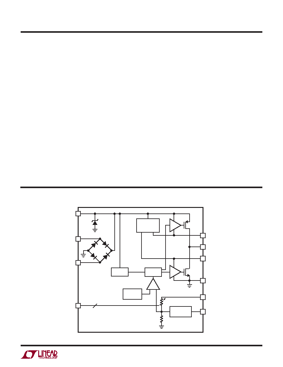
pin FuncTions
PZ1 (Pin 1): Input connection for piezoelectric element or
other AC source (used in conjunction with PZ2).
PZ2 (Pin 2): Input connection for piezoelectric element or
other AC source (used in conjunction with PZ1).
CAP (Pin 3): Internal rail referenced to VIN to serve as gate
drive for buck PMOS switch. A 1F capacitor should be
connected between CAP and VIN. This pin is not intended
for use as an external system rail.
VIN (Pin 4): Rectified Input Voltage. A capacitor on this
pin serves as an energy reservoir and input supply for the
buck regulator. The VIN voltage is internally clamped to a
maximum of 20V (typical).
SW (Pin 5): Switch Pin for the Buck Switching Regulator.
A 22H or larger inductor should be connected from SW
to VOUT.
VOUT (Pin 6): Sense pin used to monitor the output volt-
age and adjust it through internal feedback.
VIN2 (Pin 7): Internal low voltage rail to serve as gate drive
for buck NMOS switch. Also serves as a logic high rail for
output voltage select bits D0 and D1. A 4.7F capacitor
should be connected from VIN2 to GND. This pin is not
intended for use as an external system rail.
D1 (Pin 8): Output Voltage Select Bit. D1 should be tied
high to VIN2 or low to GND to select desired VOUT (see
Table 1).
D0 (Pin 9): Output Voltage Select Bit. D0 should be tied
high to VIN2 or low to GND to select desired VOUT (see
Table 1).
PGOOD (Pin 10): Power good output is logic high when
VOUT is above 92% of the target value. The logic high is
referenced to the VOUT rail.
GND (Exposed Pad Pin 11): Ground. The Exposed Pad
should be connected to a continuous ground plane on the
second layer of the printed circuit board by several vias
directly under the LTC3588-2.
block DiagraM
35882 BD
D1, D0
PZ2
PZ1
VIN
UVLO
BUCK
CONTROL
INTERNAL RAIL
GENERATION
2
BANDGAP
REFERENCE
SLEEP
PGOOD
COMPARATOR
CAP
SW
GND
PGOOD
VIN2
VOUT
20V
5
3
7
11
10
6
8, 9
2
1
4
相關(guān)PDF資料 |
PDF描述 |
|---|---|
| LTC3588IDD-2#PBF | 1-CHANNEL POWER SUPPLY SUPPORT CKT, PDSO10 |
| LTC3588IDD-1#TRPBF | SWITCHING REGULATOR, PDSO10 |
| LTC3588EDD-1#TRPBF | SWITCHING REGULATOR, PDSO10 |
| LTC3608IWKG#TRPBF | 8 A SWITCHING REGULATOR, PQCC52 |
| LTC3610IWP#TR | SWITCHING REGULATOR, PQCC64 |
相關(guān)代理商/技術(shù)參數(shù) |
參數(shù)描述 |
|---|---|
| LTC3589 | 制造商:LINER 制造商全稱:Linear Technology 功能描述:8-Output Regulator with Sequencing and I2C |
| LTC3589_1 | 制造商:LINER 制造商全稱:Linear Technology 功能描述:8-Output Regulator with Sequencing and I2C |
| LTC3589_12 | 制造商:LINEAR 制造商全稱:LINEAR 功能描述:8-Output Regulator with Sequencing and I2C |
| LTC3589-1 | 制造商:LINEAR 制造商全稱:LINEAR 功能描述:8-Output Regulator with Sequencing and I2C |
| LTC3589-2 | 制造商:LINEAR 制造商全稱:LINEAR 功能描述:8-Output Regulator with Sequencing and I2C |
發(fā)布緊急采購(gòu),3分鐘左右您將得到回復(fù)。