- 您現(xiàn)在的位置:買賣IC網(wǎng) > PDF目錄44990 > LTC3404MPMS8#TRPBF (LINEAR TECHNOLOGY CORP) 1.5 A SWITCHING REGULATOR, 1650 kHz SWITCHING FREQ-MAX, PDSO8 PDF資料下載
參數(shù)資料
| 型號: | LTC3404MPMS8#TRPBF |
| 廠商: | LINEAR TECHNOLOGY CORP |
| 元件分類: | 穩(wěn)壓器 |
| 英文描述: | 1.5 A SWITCHING REGULATOR, 1650 kHz SWITCHING FREQ-MAX, PDSO8 |
| 封裝: | LEAD FREE, PLASTIC, MSOP-8 |
| 文件頁數(shù): | 10/16頁 |
| 文件大小: | 204K |
| 代理商: | LTC3404MPMS8#TRPBF |
3
LTC3404
3404fb
Note 1: Stresses beyond those listed under Absolute Maximum Ratings
may cause permanent damage to the device. Exposure to any Absolute
Maximum Rating condition for extended periods may affect device
reliability and lifetime.
Note 2: The LTC3404E is guaranteed to meet performance specifications
from 0
°C to 85°C. Specifications over the –40°C to 85°C operating
temperature range are assured by design, characterization and correlation
with statistical process controls. The LTC3404I is guaranteed to meet
performance specifications over the –40
°C to 85°C operating temperature
range. The LTC3404MP is guaranteed to meet performance specifications
over the –55
°C to 125°C operating temperature range.
Note 3: TJ is calculated from the ambient temperature TA and power
dissipation PD according to the following formulas:
TJ = TA + (PD)(150°C/W)
Note 4: The LTC3404 is tested in a feedback loop which servos VFB to the
balance point for the error amplifier (VITH = 1.2V).
Note 5: Dynamic supply current is higher due to the gate charge being
delivered at the switching frequency.
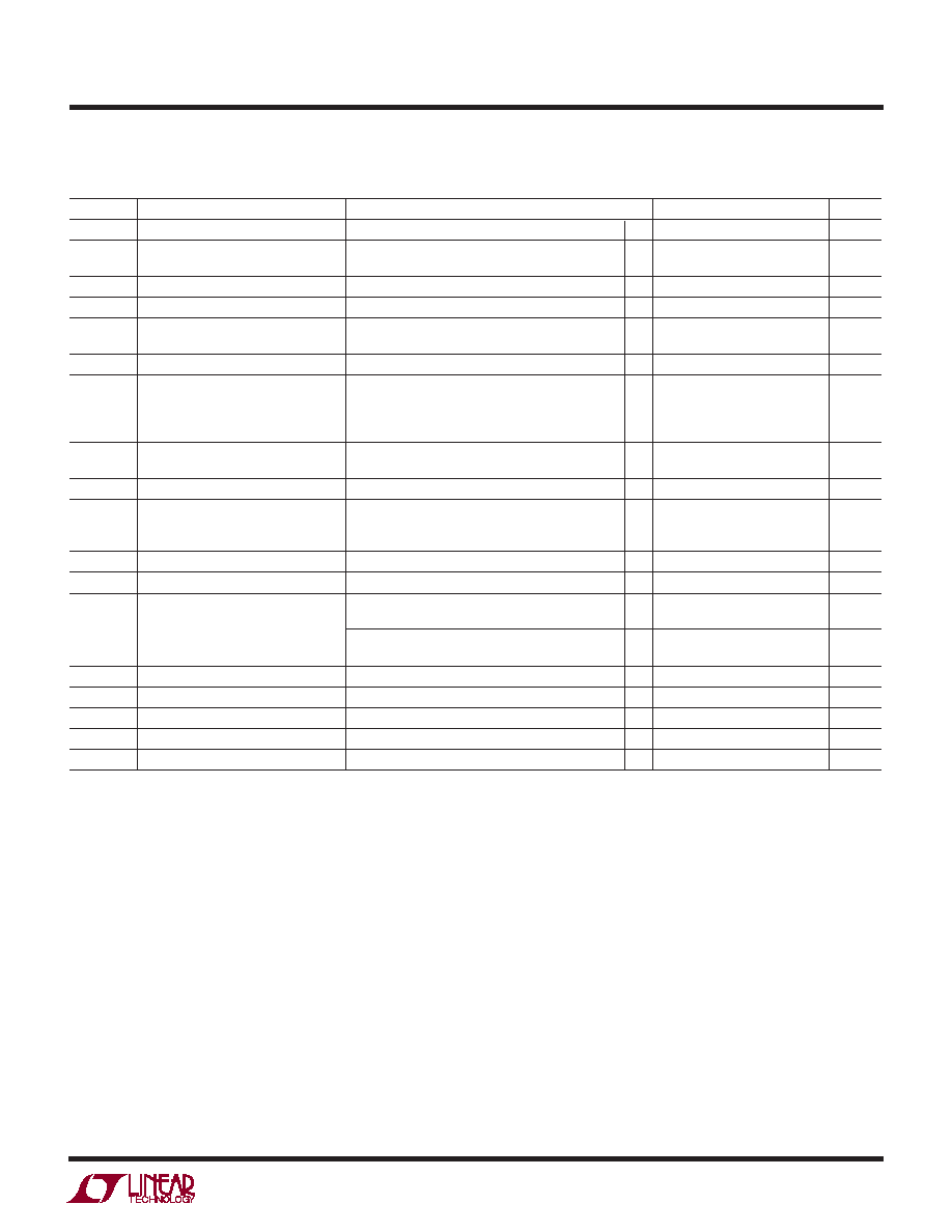
SYMBOL
PARAMETER
CONDITIONS
MIN
TYP
MAX
UNITS
IVFB
Feedback Current
(Note 4)
4
30
nA
VFB
Regulated Output Voltage
(Note 4) 0
°C ≤ TA ≤ 125°C
0.784
0.8
0.816
V
(Note 4) – 55
°C ≤ TA ≤ 125°C
0.74
0.8
0.84
V
ΔVOVL
Output Overvoltage Lockout
ΔVOVL = VOVL – VFB
20
50
110
mV
ΔVFB
Reference Voltage Line Regulation
VIN = 2.65V to 6V (Note 4)
0.05
0.2
%/V
VLOADREG
Output Voltage Load Regulation
Measured in Servo Loop; VITH = 0.9V to 1.2V
0.1
1
%
Measured in Servo Loop; VITH = 1.5V to 1.2V
– 0.1
– 1
%
VIN
Input Voltage Range
2.65
6
V
IQ
Input DC Bias Current
(Note 5)
Pulse Skipping Mode
2.65V < VIN < 6V, VSYNC/MODE = 0V, IOUT = 0A
400
700
μA
Burst Mode Operation
VSYNC/MODE = VIN, IOUT = 0A
10
15
μA
Shutdown
VRUN = 0V, VIN = 6V
0
1
μA
fOSC
Oscillator Frequency
VFB = 0.8V
1.25
1.4
1.65
MHz
VFB = 0V
200
kHz
fSYNC
SYNC Capture Range
1.0
1.7
MHz
IPLL LPF
Phase Detector Output Current
Sinking Capability
fPLLIN < fOSC
6
20
40
μA
Sourcing Capability
fPLLIN > fOSC
–6
–20
–40
μA
RPFET
RDS(ON) of P-Channel MOSFET
ISW = 100mA
0.7
Ω
RNFET
RDS(ON) of N-Channel MOSFET
ISW = –100mA
0.8
Ω
IPK
Peak Inductor Current
VIN = 3.3V, VFB = 0.7V, Duty Cycle < 35%,
0.4
1.0
1.1
A
TA = 125°C
VIN = 4V, VFB = 0.7V, Duty Cycle < 35%,
0.8
1.2
A
TA = 125°C
ILSW
SW Leakage
VRUN = 0V, VSW = 0V or 6V, VIN = 6V
±3
μA
VSYNC/MODE SYNC/MODE Threshold
VSYNC/MODE Rising
0.3
1.5
V
ISYNC/MODE
SYNC/MODE Leakage Current
±1
μA
VRUN
RUN Threshold
VRUN Rising
0.3
1.5
V
IRUN
RUN Input Current
±1
μA
The
● denotes specifications which apply over –55
°C to 125°C, otherwise specifications are TA = 25°C.
VIN = 3.6V unless otherwise specified.
ELECTRICAL CHARACTERISTICS
相關PDF資料 |
PDF描述 |
|---|---|
| LTC3404IMS8#TRPBF | 1.5 A SWITCHING REGULATOR, 1650 kHz SWITCHING FREQ-MAX, PDSO8 |
| LTC3406ABES5#PBF | 1.3 A SWITCHING REGULATOR, 1800 kHz SWITCHING FREQ-MAX, PDSO5 |
| LTC3406ABES5#TRM | 1.3 A SWITCHING REGULATOR, 1800 kHz SWITCHING FREQ-MAX, PDSO5 |
| LTC3406ABES5#TR | 1.3 A SWITCHING REGULATOR, 1800 kHz SWITCHING FREQ-MAX, PDSO5 |
| LTC3406B-2ES5#PBF | 1.3 A SWITCHING REGULATOR, 2700 kHz SWITCHING FREQ-MAX, PDSO5 |
相關代理商/技術參數(shù) |
參數(shù)描述 |
|---|---|
| LTC3405 | 制造商:LINEAR 制造商全稱:LINEAR 功能描述:Standalone 250mA Li-Ion Battery Charger in 2 × 2 DFN |
| LTC3405A | 制造商:LINER 制造商全稱:Linear Technology 功能描述:1.5MHz, 300mA Synchronous Step-Down Regulator in ThinSOT |
| LTC3405A-1.375 | 制造商:LINER 制造商全稱:Linear Technology 功能描述:1.375V, 1.5MHz, 300mA Synchronous Step-Down Regulators in ThinSOT |
| LTC3405A-1.5 | 制造商:LINER 制造商全稱:Linear Technology 功能描述:1.5V, 1.8V, 1.5MHz, 300mA Synchronous Step-Down Regulators in ThinSOT |
| LTC3405A-1.8 | 制造商:LINER 制造商全稱:Linear Technology 功能描述:1.5V, 1.8V, 1.5MHz, 300mA Synchronous Step-Down Regulators in ThinSOT |
發(fā)布緊急采購,3分鐘左右您將得到回復。