- 您現(xiàn)在的位置:買賣IC網(wǎng) > PDF目錄44990 > LTC3225EDDB-1#TRMPBF (LINEAR TECHNOLOGY CORP) 0.175 A SWITCHED CAPACITOR CONVERTER, 1500 kHz SWITCHING FREQ-MAX, PDSO10 PDF資料下載
參數(shù)資料
| 型號: | LTC3225EDDB-1#TRMPBF |
| 廠商: | LINEAR TECHNOLOGY CORP |
| 元件分類: | 穩(wěn)壓器 |
| 英文描述: | 0.175 A SWITCHED CAPACITOR CONVERTER, 1500 kHz SWITCHING FREQ-MAX, PDSO10 |
| 封裝: | 3 X 2 MM, LEAD FREE, PLASTIC, MO-229WECD-1, DFN-10 |
| 文件頁數(shù): | 8/14頁 |
| 文件大小: | 263K |
| 代理商: | LTC3225EDDB-1#TRMPBF |
LTC3225/LTC3225-1
3
3225fb
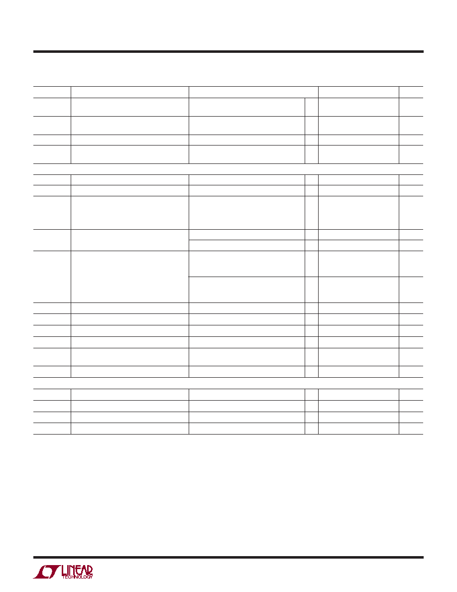
SYMBOL
PARAMETER
CONDITIONS
MIN
TYP
MAX
UNITS
VIN
Input Voltage Range
VSEL = VIN
VSEL = 0
l
2.8
5.5
V
VCOUT
Charge Termination Voltage
Sleep Mode Threshold (Rising Edge)
VSEL = VIN
VSEL = 0
l
4.4
3.9
4.5
4.0
4.6
4.1
V
VCOUT-HYS
Output Comparator Hysteresis
100
mV
VTOP/BOT
Maximum Voltage Across Each of the
Supercapacitors After Charging
VSEL = VIN
VSEL = 0
l
2.35
2.1
V
LTC3225/LTC3225-1
IQ-VIN
No Load Operating Current at VIN
IOUT = 0mA
l
20
40
μA
ISHDN-VIN
Shutdown Current
SHDN = 0V, VOUT = 0V
l
0.1
1
μA
ICOUT
COUT Leakage Current
VOUT = 5.6V, SHDN = 0V
VOUT = 5.6V, Charge Pump in Sleep Mode
VOUT = 5.6V, SHDN Connected to VIN with
Input Supply Removed
l
1
2
3
4
1
μA
IVIN
Input Charge Current
VIN = 3.6V, RPROG = 12k, CTOP = CBOT
306
mA
VIN = 3.6V, RPROG = 60k, CTOP = CBOT
55
mA
IOUT
Output Charge Current
VIN = 3.6V, RPROG = 12k, CTOP = CBOT,
VOUT = 4.5V (LTC3225),
VOUT = 3.7V (LTC3225-1)
125
150
175
mA
VIN = 3.6V, RPROG = 60k, CTOP = CBOT,
VOUT = 4.5V (LTC3225),
VOUT = 3.7V (LTC3225-1)
26
mA
VPGOOD
PGOOD Low Output Voltage
IPGOOD = –1.6mA
l
0.4
V
IPGOOD-LEAK
PGOOD High Impedance Leakage Current
VPGOOD = 5V
l
10
μA
VPG
PGOOD Low-to-High Threshold
Relative to Output Voltage Threshold
l
92
94
96
%
VPG-HYS
PGOOD Threshold Hysteresis
Relative to Output Voltage Threshold
l
0.25
1.2
2.5
%
ROL
Effective Open-Loop Output Impedance
(Note 4)
VIN = 3.6V, VOUT = 4.5V (LTC3225)
VIN = 3.6V, VOUT = 3.7V (LTC3225-1)
8
9
Ω
fOSC
CLK Frequency
l
0.6
0.9
1.5
MHz
VSEL, SHDN
VIH
Input High Voltage
l
1.3
V
VIL
Input Low Voltage
l
0.4
V
IIH
Input High Current
l
–1
1
μA
IIL
Input Low Current
l
–1
1
μA
ELECTRICAL CHARACTERISTICS The l denotes the specications which apply over the full operating
temperature range, otherwise specications are at TA = 25°C. VIN = 3.6V, CIN = 2.2μF, CFLY = 1μF, unless otherwise specied (Note 3).
Note 1: Stresses beyond those listed under Absolute Maximum Ratings
may cause permanent damage to the device. Exposure to any Absolute
Maximum Rating condition for extended periods may affect device
reliability and lifetime.
Note 2: Based on long-term current density limitations.
Note 3: The LTC3225/LTC3225-1 are tested under pulsed load conditions
such that TJ ≈ TA. The LTC3225/LTC3225-1 are guaranteed to meet
performance specications from 0°C to 85°C. Specications over the
–40°C to 85°C operating temperature range are assured by design,
characterization and correlation with statistical process controls.
Note 4: Output not in regulation;
ROL ≡ (2 VIN – VOUT)/IOUT
相關PDF資料 |
PDF描述 |
|---|---|
| LTC3226IUD#TRPBF | SWITCHED CAPACITOR REGULATOR, PQCC16 |
| LTC3226EUD#TRPBF | SWITCHED CAPACITOR REGULATOR, PQCC16 |
| LTC3226IUD#PBF | SWITCHED CAPACITOR REGULATOR, PQCC16 |
| LTC3400BES6#PBF | 0.85 A SWITCHING REGULATOR, 1500 kHz SWITCHING FREQ-MAX, PDSO6 |
| LTC3404MPMS8#PBF | 1.5 A SWITCHING REGULATOR, 1650 kHz SWITCHING FREQ-MAX, PDSO8 |
相關代理商/技術參數(shù) |
參數(shù)描述 |
|---|---|
| LTC3225EDDB-TRMPBF | 制造商:LINER 制造商全稱:Linear Technology 功能描述:150mA Supercapacitor Charger |
| LTC3225EDDB-TRPBF | 制造商:LINER 制造商全稱:Linear Technology 功能描述:150mA Supercapacitor Charger |
| LTC3226 | 制造商:LINER 制造商全稱:Linear Technology 功能描述:2-Cell Supercapacitor Charger |
| LTC3226_12 | 制造商:LINEAR 制造商全稱:LINEAR 功能描述:2-Cell Supercapacitor Charger with Backup |
| LTC3226EUD | 制造商:LINEAR 制造商全稱:LINEAR 功能描述:2-Cell Supercapacitor Charger with Backup PowerPath Controller |
發(fā)布緊急采購,3分鐘左右您將得到回復。