- 您現(xiàn)在的位置:買賣IC網(wǎng) > PDF目錄44990 > LTC3108IDE-1#PBF (LINEAR TECHNOLOGY CORP) SWITCHING REGULATOR, PDSO12 PDF資料下載
參數(shù)資料
| 型號(hào): | LTC3108IDE-1#PBF |
| 廠商: | LINEAR TECHNOLOGY CORP |
| 元件分類: | 穩(wěn)壓器 |
| 英文描述: | SWITCHING REGULATOR, PDSO12 |
| 封裝: | 4 X 3 MM, LEAD FREE, PLASTIC, MO-229WGED, DFN-12 |
| 文件頁(yè)數(shù): | 22/24頁(yè) |
| 文件大小: | 1593K |
| 代理商: | LTC3108IDE-1#PBF |
第1頁(yè)第2頁(yè)第3頁(yè)第4頁(yè)第5頁(yè)第6頁(yè)第7頁(yè)第8頁(yè)第9頁(yè)第10頁(yè)第11頁(yè)第12頁(yè)第13頁(yè)第14頁(yè)第15頁(yè)第16頁(yè)第17頁(yè)第18頁(yè)第19頁(yè)第20頁(yè)第21頁(yè)當(dāng)前第22頁(yè)第23頁(yè)第24頁(yè)
LTC3108-1
31081f
VAUX (Pin 1/Pin 2): Output of the Internal Rectifier Cir-
cuit and VCC for the IC. Bypass VAUX with at least 1F of
capacitance. An active shunt regulator clamps VAUX to
5.25V (typical).
VSTORE (Pin 2/Pin 3): Output for the Storage Capacitor
or Battery. A large capacitor may be connected from this
pin to GND for powering the system in the event the input
voltage is lost. It will be charged up to the maximum VAUX
clamp voltage. If not used, this pin should be left open
or tied to VAUX.
VOUT (Pin 3/Pin 4): Main Output of the Converter. The
voltage at this pin is regulated to the voltage selected by
VS1 and VS2 (see Table 1). Connect this pin to an energy
storage capacitor or to a rechargeable battery.
VOUT2 (Pin 4/Pin 5): Switched Output of the Converter.
Connect this pin to a switched load. This output is open
until VOUT2_EN is driven high, then it is connected to
VOUT through a 1.3 P-channel switch. If not used, this
pin should be left open or tied to VOUT. The peak current
in this output is limited to 0.3A typical.
VLDO (Pin 5/Pin 6): Output of the 2.2V LDO. Connect a
2.2F or larger ceramic capacitor from this pin to GND.
If not used, this pin should be tied to VAUX.
PGD (Pin 6/Pin 7): Power Good Output. When VOUT is
within 7.5% of its programmed value, PGD will be pulled
up to VLDO through a 1MΩ resistor. If VOUT drops 9%
below its programmed value PGD will go low. This pin
can sink up to 100A.
VS2 (Pin 7/Pin 10): VOUT Select Pin 2. Connect this pin
to ground or VAUX to program the output voltage (see
Table 1).
VS1 (Pin 8/Pin 11): VOUT Select Pin 1. Connect this pin
to ground or VAUX to program the output voltage (see
Table 1).
VOUT2_EN (Pin 9/Pin 12): Enable Input for VOUT2. VOUT2
will be enabled when this pin is driven high. There is an
internal 5M pull-down resistor on this pin. If not used,
this pin can be left open or grounded.
C1(Pin10/Pin13):InputtotheChargePumpandRectifier
Circuit. Connect a capacitor from this pin to the secondary
winding of the step-up transformer.
C2 (Pin 11/Pin 14): Input to the N-Channel Gate Drive
Circuit. Connect a capacitor from this pin to the secondary
winding of the step-up transformer.
SW (Pin 12/Pin 15): Drain of the Internal N-Channel
Switch. Connect this pin to the primary winding of the
transformer.
GND (Pins 1, 8, 9, 16) SSOP Only: Ground
GND (Exposed Pad Pin 13) DFN Only: Ground. The DFN
exposed pad must be soldered to the PCB ground plane.
It serves as the ground connection, and as a means of
conducting heat away from the die.
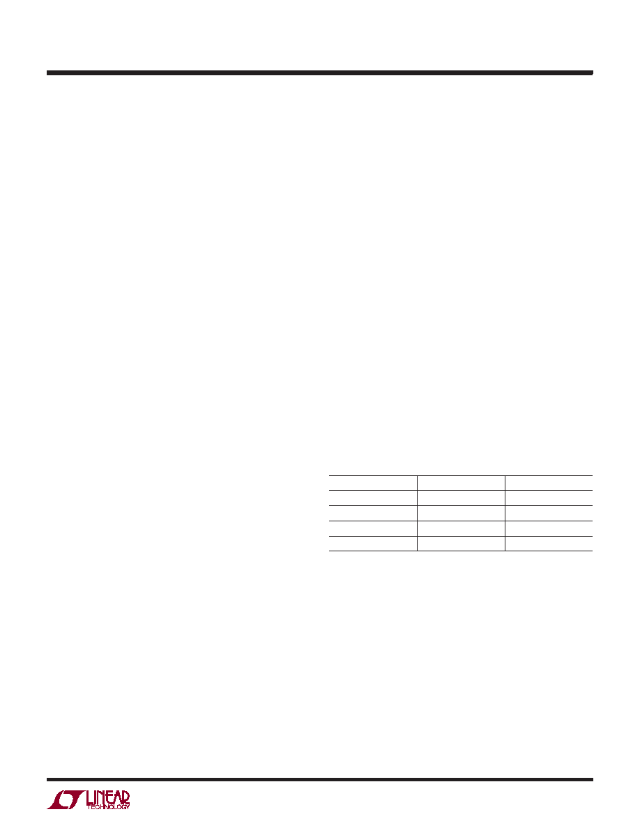
Table 1. Regulated Voltage Using Pins VS1 and VS2
VS2
VS1
VOUT
GND
2.5V
GND
VAUX
3V
VAUX
GND
3.7V
VAUX
4.5V
pin FuncTions (DFN/SSOP)
相關(guān)PDF資料 |
PDF描述 |
|---|---|
| LTC3108IGN-1#PBF | SWITCHING REGULATOR, PDSO12 |
| LTC3108EGN-1#TRPBF | SWITCHING REGULATOR, PDSO12 |
| LTC3108EDE-1#PBF | SWITCHING REGULATOR, PDSO12 |
| LTC3112IDHD#PBF | 12 A SWITCHING REGULATOR, 825 kHz SWITCHING FREQ-MAX, PDSO16 |
| LTC3112IFE#PBF | 12 A SWITCHING REGULATOR, 825 kHz SWITCHING FREQ-MAX, PDSO20 |
相關(guān)代理商/技術(shù)參數(shù) |
參數(shù)描述 |
|---|---|
| LTC3108IDE-1-TRPBF | 制造商:LINER 制造商全稱:Linear Technology 功能描述:Ultralow Voltage Step-Up Converter and Power Manager |
| LTC3108IDEPBF | 制造商:LINER 制造商全稱:Linear Technology 功能描述:Ultralow Voltage Step-Up Converter and Power Manager |
| LTC3108IDE-PBF | 制造商:LINER 制造商全稱:Linear Technology 功能描述:Ultralow Voltage Step-Up Converter and Power Manager |
| LTC3108IDETRPBF | 制造商:LINER 制造商全稱:Linear Technology 功能描述:Ultralow Voltage Step-Up Converter and Power Manager |
| LTC3108IDE-TRPBF | 制造商:LINER 制造商全稱:Linear Technology 功能描述:Ultralow Voltage Step-Up Converter and Power Manager |
發(fā)布緊急采購(gòu),3分鐘左右您將得到回復(fù)。