- 您現(xiàn)在的位置:買(mǎi)賣(mài)IC網(wǎng) > PDF目錄299419 > LTC1061MJ (LINEAR TECHNOLOGY CORP) High Performance Triple Universal Filter Building Block PDF資料下載
參數(shù)資料
| 型號(hào): | LTC1061MJ |
| 廠商: | LINEAR TECHNOLOGY CORP |
| 元件分類: | 模擬濾波器 |
| 英文描述: | High Performance Triple Universal Filter Building Block |
| 中文描述: | TRIPLE SWITCHED CAPACITOR FILTER, RESISTOR PROGRAMMABLE, UNIVERSAL, CDIP20 |
| 封裝: | 0.300 INCH, CERAMIC, DIP-20 |
| 文件頁(yè)數(shù): | 12/16頁(yè) |
| 文件大?。?/td> | 325K |
| 代理商: | LTC1061MJ |
第1頁(yè)第2頁(yè)第3頁(yè)第4頁(yè)第5頁(yè)第6頁(yè)第7頁(yè)第8頁(yè)第9頁(yè)第10頁(yè)第11頁(yè)當(dāng)前第12頁(yè)第13頁(yè)第14頁(yè)第15頁(yè)第16頁(yè)
5
LTC1061
1061fe
DESCRIPTIO A D
U
PI
U
APPLICATIO
U
HI TS
U
–
+
Σ
+
∫
Σ
LEVEL
SHIFT
LEVEL
SHIFT
LEVEL
SHIFT
CLOCK
GENERATOR
CLOCK
GENERATOR
CLOCK
GENERATOR
CLK
(8)
LEVEL SHIFT
(9)
TO FILTER A
TO FILTER B
TO FILTER C
+
∫
+
∫
+
∫
+
∫
+
∫
50/100/
HOLD
(7)
AGND
(6)
V+
(10)
V –
(15)
HPC
(12)
S1B
(16)
BPC
(13)
LPC
(14)
S1A
(5)
NB
(18)
BPB
(19)
LPB
(20)
NA
(3)
BPA
(2)
LPA
(1)
INVA
(4)
INVB
(17)
INVC
(11)
1061 BD
+
–
+
–
+
–
+
frequencies below 500kHz the clock “on” time can be as
low as 300ns. The maximum clock frequency for
±5V
supplies and above is 2.4MHz.
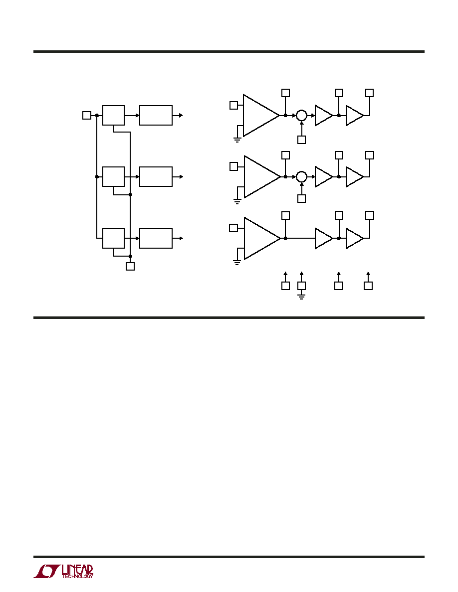
S1A, S1B (Pins 5, 16)
These are voltage input pins. If used, they should be driven
with a source impedance below 5k
. when they are not
used, they should be tied to the analog ground Pin 6.
AGND (Pin 6)
When the LTC1061 operates with dual supplies, Pin 6
should be tied to system ground. When the LTC1061
operates with a single positive supply, the analog ground
pin should be tied to 1/2 supply, Figure 1. The positive
input of all the internal op amps, as well as the common
reference of all the internal switches, are internally tied to
the analog ground pin. Because of this, a “clean” ground
is recommended.
Power Supplies (Pins 10, 15)
They should be bypassed with 0.1
F disc ceramic. Low
noise, nonswitching, power supplies are recommended.
The device operates with a single 5V supply, Figure 1, and
with dual supplies. The absolute maximum operating
power supply voltage is
±9V.
Clock and Level shift (Pins 8, 9)
When the LTC1061 operates with symmetrical dual sup-
plies the level shift Pin 9 should be tied to analog ground.
For single 5V supply operation, the level shift pin should be
tied to Pin 15 which will be the system ground. The typical
logic threshold levels of the clock pin are as follows: 1.65V
above the level shift pin for
±5V supply operation, 1.75V
for
±7.5V and above, and 1.4V for single 5V supply
operation. The logic threshold levels vary
±100mV over
the full military temperature range. The recommended
duty cycle of the input clock is 50% although for clock
BLOCK DIAGRA
W
相關(guān)PDF資料 |
PDF描述 |
|---|---|
| LTC1061AM | High Performance Triple Universal Filter Building Block |
| LTC1061C | High Performance Triple Universal Filter Building Block |
| LTC1061M | High Performance Triple Universal Filter Building Block |
| LTC1061CS | High Performance Triple Universal Filter Building Block |
| LTC1061S | High Performance Triple Universal Filter Building Block |
相關(guān)代理商/技術(shù)參數(shù) |
參數(shù)描述 |
|---|---|
| LTC1061MJ/883 | 制造商:Linear Technology 功能描述:Active Filter Triple SW-CAP UNIV 6th Order 35kHz 20-Pin CDIP |
| LTC1061MJ/883B | 制造商:未知廠家 制造商全稱:未知廠家 功能描述:Analog Filter |
| LTC1061S | 制造商:LINER 制造商全稱:Linear Technology 功能描述:High Performance Triple Universal Filter Building Block |
| LTC1062 | 制造商:LINER 制造商全稱:Linear Technology 功能描述:5th Order Lowpass Filter |
| LTC1062_09 | 制造商:LINER 制造商全稱:Linear Technology 功能描述:5th Order Lowpass Filter |
發(fā)布緊急采購(gòu),3分鐘左右您將得到回復(fù)。