- 您現(xiàn)在的位置:買賣IC網(wǎng) > PDF目錄299419 > LTC1061M (Linear Technology Corporation) High Performance Triple Universal Filter Building Block PDF資料下載
參數(shù)資料
| 型號(hào): | LTC1061M |
| 廠商: | Linear Technology Corporation |
| 英文描述: | High Performance Triple Universal Filter Building Block |
| 中文描述: | 三高性能通用濾波器積木 |
| 文件頁(yè)數(shù): | 15/16頁(yè) |
| 文件大小: | 352K |
| 代理商: | LTC1061M |
第1頁(yè)第2頁(yè)第3頁(yè)第4頁(yè)第5頁(yè)第6頁(yè)第7頁(yè)第8頁(yè)第9頁(yè)第10頁(yè)第11頁(yè)第12頁(yè)第13頁(yè)第14頁(yè)當(dāng)前第15頁(yè)第16頁(yè)
8
LTC1061
ODES OF OPERATIO
W
U
Figure 6. Measures Frequency Response of
the Lowpass Butterworth Filter of Figure 3.
2. Secondary Modes: Mode 1b – It is derived from Mode
1. In Mode 1b, Figure 7, two additional resistors, R5 and
R6, are added to attenuate the amount of voltage fed back
from the lowpass output into the input of the SA (SB)
switched capacitor summer. This allows the filter clock-
to-center frequency ratio to be adjusted beyond 50:1 (or
100:1). Mode 1b still maintains the speed advantages of
Mode 1. Figure 8 shows the 3 lowpass sections of the
LTC1061 in cascade resulting in a Chebyshev lowpass
filter. The side A of the IC is connected in Mode 1b to
provide the first resonant frequency below the cutoff
frequency of the filter. The practical ripple, obtained by
using a non-A version of the LTC1061 and 1% standard
resistor values, was 0.15dB. For this 6th order lowpass,
the textbook Qs and center frequencies normalized to the
ripple bandwidth are: Q1 = 0.55, fO1 = 0.71, Q2 = 1.03, FO2
= 0.969, Q3 = 3.4, FO3 = 1.17. The design was done with
speed in mind. The higher (Q3, FO3) section was in Mode
1 and placed in the side B of the LTC1061. The remaining
two center frequencies were then normalized with respect
to the center frequency of side B; this changes the ratio of
clock-to-cutoff frequency from 50:1 to 50
× 1.17 = 58.5:1.
As shown in Figure 9, the maximum cutoff frequency is
about 33kHz. The total wideband output noise is 220
VRMS
and the measured output DC offset voltage is 60mV.
–
+
Σ
∫
AGND
R1
N
BP
LP
VIN
1061 F07
+
–
S
R2
R3
R6
R5
fO =
; fn = fO; Q =
HON1 (f → 0) = HON2
= –
HOLP =
; HOBP = –
; (R5//R6) <5k
fCLK
100(50)
R2
R1
R3
R2
–R2/R1
R6/(R5 + R6)
R3
R1
√ R6
R5 + R6
√ R6
R5 + R6
fCLK
2
f
→
()
fIN (Hz)
10k
–70
V
OUT
/V
IN
(dB)
–60
–50
–40
–30
100k
1M
1061 F09
–20
–10
0
30k
VS > ±5V
TA = 25°C
VIN = 1VRMS
fCLK = 1.9MHz
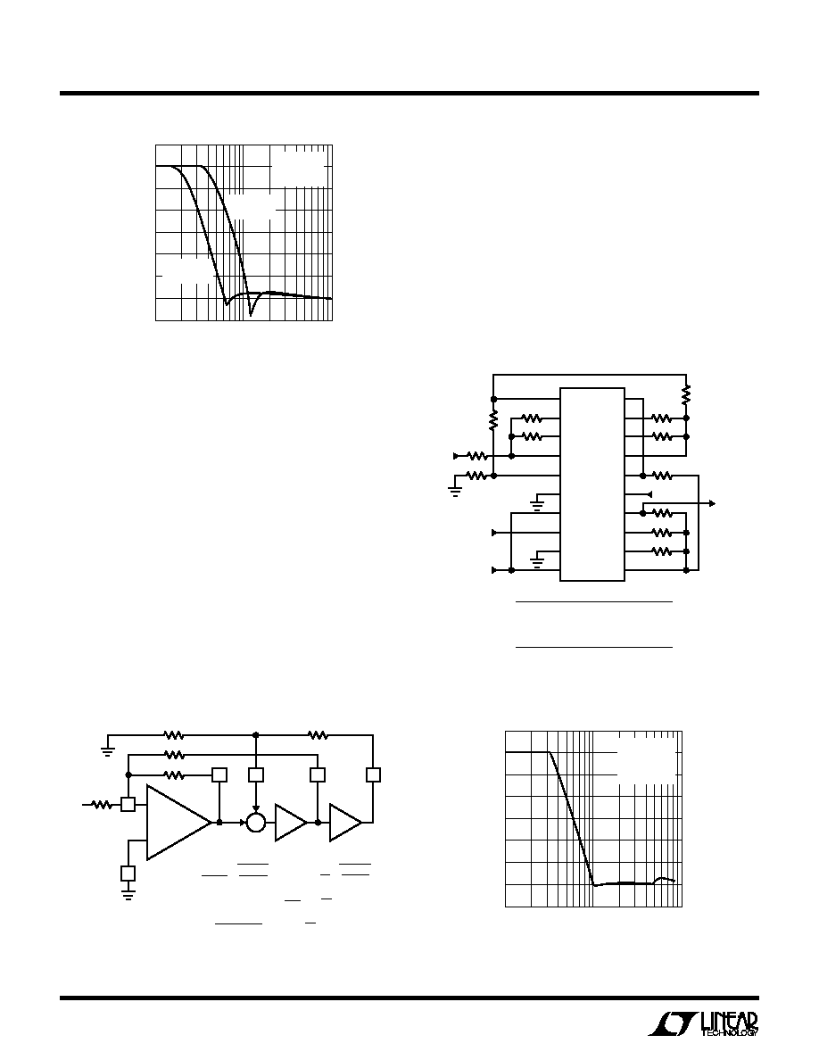
Figure 8. 6th Order Chebyshev, Lowpass Filter Using 3
Different Modes of Operation for Speed Optimization
Figure 9. Amplitude Response of the 6th Order
Chebyshev Lowpass Filter of Figure 8
Figure 7. Mode 1b: 2nd Order Filter Providing
Notch, Bandpass, Lowpass
fIN (Hz)
10k
–70
GAIN
(dB)
–60
–50
–40
–30
100k
1M
1061 F06
–20
–10
0
20k
40k
200k
VS ≥ ±5V
TA = 25°C
VIN = 1VRMS
fCLK = 2MHz
fC = 40kHz
fCLK = 1MHz
fC = 20kHz
20
19
18
17
16
15
14
13
12
11
1
2
3
4
5
6
7
8
9
10
R32
VOUT
R11
VIN
LTC1061 F08
LTC1061
R22
R12
R33
R23
R43
R31
R21
fCLK < 2MHz
V –
R13
V+
R51
R61
STANDARD 1% RESISTOR VALUES
R11 = 35.7k
R31 = 11.5k
R51 = 5.49k
R12 = 11k
R61 = 2.87k
R22 = 11k
R23 = 10.5
R43 = 15.8k
R32 = 36.5k
R13 = 15.8k
R33 = 13k
R21 = 12.1k
相關(guān)PDF資料 |
PDF描述 |
|---|---|
| LTC1061CS | High Performance Triple Universal Filter Building Block |
| LTC1061S | High Performance Triple Universal Filter Building Block |
| LTC1062CJ8 | 5th Order Lowpass Filter |
| LTC1062MJ8 | 5th Order Lowpass Filter |
| LTC1062CS | 5th Order Lowpass Filter |
相關(guān)代理商/技術(shù)參數(shù) |
參數(shù)描述 |
|---|---|
| LTC1061MJ | 制造商:LINER 制造商全稱:Linear Technology 功能描述:High Performance Triple Universal Filter Building Block |
| LTC1061MJ/883 | 制造商:Linear Technology 功能描述:Active Filter Triple SW-CAP UNIV 6th Order 35kHz 20-Pin CDIP |
| LTC1061MJ/883B | 制造商:未知廠家 制造商全稱:未知廠家 功能描述:Analog Filter |
| LTC1061S | 制造商:LINER 制造商全稱:Linear Technology 功能描述:High Performance Triple Universal Filter Building Block |
| LTC1062 | 制造商:LINER 制造商全稱:Linear Technology 功能描述:5th Order Lowpass Filter |
發(fā)布緊急采購(gòu),3分鐘左右您將得到回復(fù)。