- 您現(xiàn)在的位置:買賣IC網(wǎng) > PDF目錄44987 > LT6107MPS5#TR (LINEAR TECHNOLOGY CORP) SPECIALTY ANALOG CIRCUIT, PDSO5 PDF資料下載
參數(shù)資料
| 型號: | LT6107MPS5#TR |
| 廠商: | LINEAR TECHNOLOGY CORP |
| 元件分類: | 模擬信號調(diào)理 |
| 英文描述: | SPECIALTY ANALOG CIRCUIT, PDSO5 |
| 封裝: | PLASTIC, MO-193, TSOT-23, 5 PIN |
| 文件頁數(shù): | 12/12頁 |
| 文件大小: | 279K |
| 代理商: | LT6107MPS5#TR |
LT6107
9
6107fb
APPLICATIONS INFORMATION
Output Error Due to the Amplier DC Offset
Voltage, VOS
EV
R
OUT VOS
OS
OUT
IN
()
=
The DC offset voltage of the amplier adds directly to the
value of the sense voltage, VSENSE. This is the dominant
error of the system and it limits the low end of the dynamic
range. The paragraph “Selection of External Current Sense
Resistor” provides details.
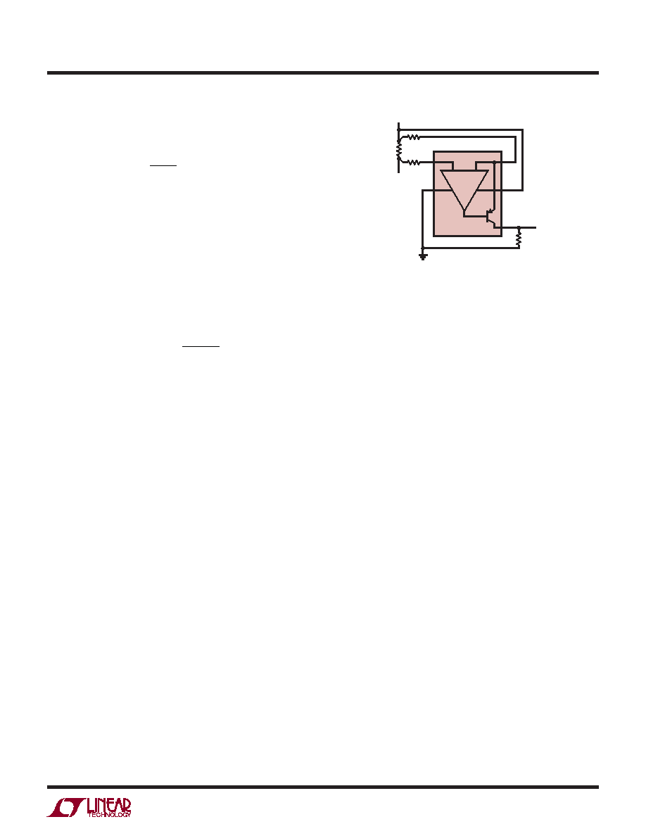
Output Error Due to the Bias Currents, IB+ and IB–
The bias current IB+ ows into the positive input of the
internal op amp. IB– ows into the negative input.
EOUT(IBIAS) = ROUT IB
+ RSENSE
RIN
–IB
–
Assuming IB+ IB– = IBIAS, and RSENSE << RIN then:
EOUT(IBIAS) –ROUT IBIAS
It is convenient to refer the error to the input:
EIN(IBIAS) –RIN IBIAS
For instance if IBIAS is 60nA and RIN is 1k, the input referred
error is 60μV. Note that in applications where RSENSE RIN,
IB+ causes a voltage offset in RSENSE that cancels the er-
ror due to IB– and EOUT(IBIAS) 0mV. In most applications,
RSENSE << RIN, the bias current error can be similarly re-
duced if an external resistor RIN+ = (RIN – RSENSE) is con-
nected as shown in Figure 4. Under both conditions:
EIN(IBIAS) = ±RIN IOS; where IOS = IB+ – IB–
If the offset current, IOS, of the LT6107 amplier is 6nA,
the 60μV error above is reduced to 6μV.
Adding RIN+ as described will maximize the dynamic
range of the circuit. For less sensitive designs, RIN+ is
not necessary.
Output Error Due to Gain Error
The LT6107 exhibits a typical gain error of –0.25% at 1mA
output current. The primary source of gain error is due to
the nite gain to the PNP output transistor, which results in
a small percentage of the current in RIN not appearing in the
output load ROUT.
Minimum Output Voltage
The curves of the Output Voltage vs Input Sense Voltage
show the behavior of the LT6107 with low input sense volt-
ages. When VSENSE = 0V, the output voltage will always
be slightly positive, the result of input offset voltages and
of a small amount of quiescent current (0.7μA to 1.2μA)
owing through the output device. The minimum output
voltage in the Electrical Characteristics table include both
these effects.
Power Dissipation Considerations
The power dissipated by the LT6107 will cause a small
increase in the die temperature. This rise in junction tem-
perature can be calculated if the output current and the
supply current are known.
The power dissipated in the LT6107 due to the output
signal is:
POUT = (V–IN – VOUT) IOUT
Since V–IN V+, POUT (V+ – VOUT) IOUT
The power dissipated due to the quiescent supply current is:
PQ = IS (V+ – V–)
The total power dissipated is the output dissipation plus
the quiescent dissipation:
PTOTAL = POUT + PQ
The junction temperature is given by:
TJ = TA + θJA PTOTAL
At the maximum operating supply voltage of 36V and the
maximum guaranteed output current of 1mA, the total
Figure 4. Second Input R Minimizes Error Due to Input Bias Current
LT6107
ROUT
VOUT
6107 F04
RIN
–
RIN
+
V+
LOAD
RSENSE
–
+
V+
V–
OUT
RIN
+ = RIN– – RSENSE
–IN
+IN
相關(guān)PDF資料 |
PDF描述 |
|---|---|
| LT6107MPS5#TRM | SPECIALTY ANALOG CIRCUIT, PDSO5 |
| LT6109IMS-1#PBF | SPECIALTY ANALOG CIRCUIT, PDSO10 |
| LT6109HMS-1#TRPBF | SPECIALTY ANALOG CIRCUIT, PDSO10 |
| LT6555IGN#PBF | TRIPLE 1-CHANNEL, VIDEO MULTIPLEXER, PDSO24 |
| LT6604CUFF-2.5#PBF | SPECIALTY ANALOG CIRCUIT, PQCC34 |
相關(guān)代理商/技術(shù)參數(shù) |
參數(shù)描述 |
|---|---|
| LT6107MPS5-TRM | 制造商:LINER 制造商全稱:Linear Technology 功能描述:High Temperature High Side Current Sense Amp in SOT-23 |
| LT6107MPS5-TRMPBF | 制造商:LINER 制造商全稱:Linear Technology 功能描述:High Temperature High Side Current Sense Amp in SOT-23 |
| LT6107MPS5-TRPBF | 制造商:LINER 制造商全稱:Linear Technology 功能描述:High Temperature High Side Current Sense Amp in SOT-23 |
| LT6108AHMS-1#PBF | 制造商:Linear Technology 功能描述:SC-Amps/Current Sense, High Side Current Sense Amplifier with Reference and Comp |
| LT6108AHMS-1#TRPBF | 制造商:Linear Technology 功能描述:SC-Amps/Current Sense, High Side Current Sense Amplifier with Reference and Comp |
發(fā)布緊急采購,3分鐘左右您將得到回復(fù)。