- 您現(xiàn)在的位置:買賣IC網(wǎng) > PDF目錄30766 > LT1228IS8#TR (LINEAR TECHNOLOGY CORP) 1 CHANNEL, VIDEO AMPLIFIER, PDSO8 PDF資料下載
參數(shù)資料
| 型號(hào): | LT1228IS8#TR |
| 廠商: | LINEAR TECHNOLOGY CORP |
| 元件分類: | 音頻/視頻放大 |
| 英文描述: | 1 CHANNEL, VIDEO AMPLIFIER, PDSO8 |
| 封裝: | 0.150 INCH, PLASTIC, SOP-8 |
| 文件頁(yè)數(shù): | 15/20頁(yè) |
| 文件大小: | 401K |
| 代理商: | LT1228IS8#TR |
第1頁(yè)第2頁(yè)第3頁(yè)第4頁(yè)第5頁(yè)第6頁(yè)第7頁(yè)第8頁(yè)第9頁(yè)第10頁(yè)第11頁(yè)第12頁(yè)第13頁(yè)第14頁(yè)當(dāng)前第15頁(yè)第16頁(yè)第17頁(yè)第18頁(yè)第19頁(yè)第20頁(yè)
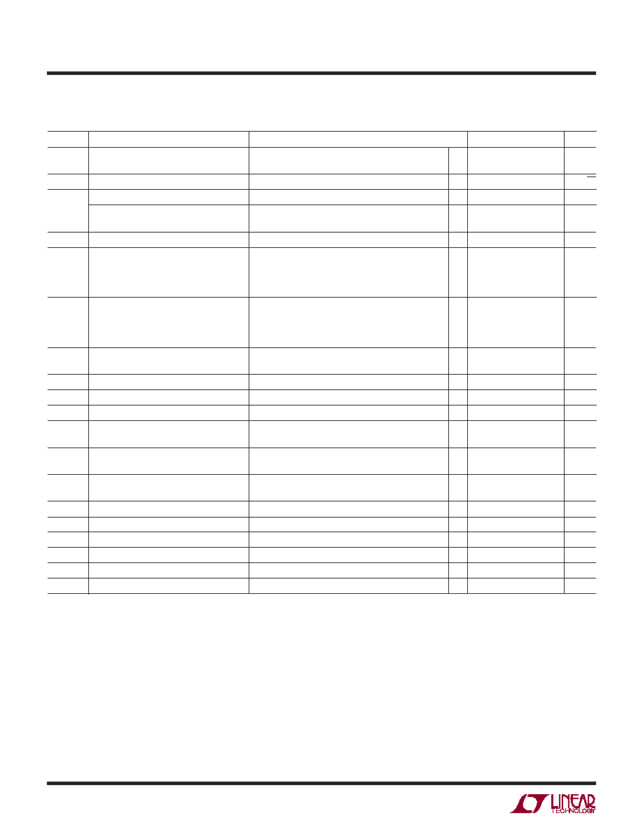
4
LT1228
1228fc
IB
Input Bias Current
TA = 25°C
0.4
1
A
●
5
A
en
Input Noise Voltage Density
f = 1kHz
20
nV/
√Hz
RIN
Input Resistance-Differential Mode
VIN ≈ ±30mV
●
30
200
k
Input Resistance-Common Mode
VS = ±15V, VCM = ±12V
●
50
1000
M
VS = ±5V, VCM = ±2V
●
50
1000
M
CIN
Input Capacitance
3pF
Input Voltage Range
VS = ±15V, TA = 25°C
±13
±14
V
VS = ±15V
●
±12
V
VS = ±5V, TA = 25°C
±3
±4V
VS = ±5V
●
±2V
CMRR
Common Mode Rejection Ratio
VS = ±15V, VCM = ±13V, TA = 25°C
60
100
dB
VS = ±15V, VCM = ±12V
●
60
dB
VS = ±5V, VCM = ±3V, TA = 25°C
60
100
dB
VS = ±5V, VCM = ±2V
●
60
dB
PSRR
Power Supply Rejection Ratio
VS = ±2V to ±15V, TA = 25°C
60
100
dB
VS = ±3V to ±15V
●
60
dB
gm
Transconductance
ISET = 100A, IOUT = ±30A, TA = 25°C
0.75
1.00
1.25
A/mV
Transconductance Drift
●
– 0.33
%/
°C
IOUT
Maximum Output Current
ISET = 100A
●
70
100
130
A
IOL
Output Leakage Current
ISET = 0A (+IIN of CFA), TA = 25°C
0.3
3
A
●
10
A
VOUT
Maximum Output Voltage Swing
VS = ±15V , R1 = ∞
● ±13
±14
V
VS = ±5V , R1 = ∞
● ±3
±4V
RO
Output Resistance
VS = ±15V, VOUT = ±13V
●
28
M
VS = ±5V, VOUT = ±3V
●
28
M
Output Capacitance (Note 3)
VS = ±5V
6
pF
IS
Supply Current, Both Amps
ISET = 1mA
●
915
mA
THD
Total Harmonic Distortion
VIN = 30mVRMS at 1kHz, R1 = 100k
0.2
%
BW
Small-Signal Bandwidth
R1 = 50
,ISET = 500A
80
MHz
tr
Small-Signal Rise Time
R1 = 50
,ISET = 500A, 10% to 90%
5
ns
Propagation Delay
R1 = 50
,ISET = 500A, 50% to 50%
5
ns
ELECTRICAL C
C
HARA TERISTICS
SYMBOL
PARAMETER
CONDITIONS
MIN
TYP
MAX
UNITS
Note 1: Stresses beyond those listed under Absolute Maximum Ratings
may cause permanent damage to the device. Exposure to any Absolute
Maximum Rating condition for extended periods may affect device
reliability and lifetime.
Note 2: A heat sink may be required depending on the power supply
voltage.
Note 3: This is the total capacitance at Pin 1. It includes the input
capacitance of the current feedback amplifier and the output capacitance
of the transconductance amplifier.
Note 4: Slew rate is measured at
±5V on a ±10V output signal while
operating on
±15V supplies with RF = 1k, RG = 110 and RL = 400. The
slew rate is much higher when the input is overdriven, see the applications
section.
Note 5: Rise time is measured from 10% to 90% on a
±500mV output
signal while operating on
±15V supplies with RF = 1k, RG = 110 and
RL = 100. This condition is not the fastest possible, however, it does
guarantee the internal capacitances are correct and it makes automatic
testing practical.
Note 6: AC parameters are 100% tested on the ceramic and plastic DIP
packaged parts (J and N suffix) and are sample tested on every lot of
the SO packaged parts (S suffix).
Note 7: NTSC composite video with an output level of 2V.
Note 8: Back to back 6V Zener diodes are connected between Pins 2
and 3 for ESD protection.
The
● denotes the specifications which apply over the full operating
temperature range, otherwise specifications are at TA = 25°C. Transconductance Amplifier, Pins 1, 2, 3, 5. ±5V ≤ VS ≤ ±15V, ISET =
100
A, VCM = 0V unless otherwise noted.
相關(guān)PDF資料 |
PDF描述 |
|---|---|
| LT1228MJ8#PBF | 1 CHANNEL, VIDEO AMPLIFIER, CDIP8 |
| LT1228MJ8#TRPBF | 1 CHANNEL, VIDEO AMPLIFIER, CDIP8 |
| LT1228MJ8#TR | 1 CHANNEL, VIDEO AMPLIFIER, CDIP8 |
| LT1304CS8-3.3#PBF | 1.2 A SWITCHING REGULATOR, 300 kHz SWITCHING FREQ-MAX, PDSO8 |
| LT1304CS8-3.3#TRPBF | 1.2 A SWITCHING REGULATOR, 300 kHz SWITCHING FREQ-MAX, PDSO8 |
相關(guān)代理商/技術(shù)參數(shù) |
參數(shù)描述 |
|---|---|
| LT1228M | 制造商:LINER 制造商全稱:Linear Technology 功能描述:100MHz Current Feedback Amplifier with DC Gain Control |
| LT1228MJ8 | 制造商:LINER 制造商全稱:Linear Technology 功能描述:100MHz Current Feedback Amplifier with DC Gain Control |
| LT1229 | 制造商:LINER 制造商全稱:Linear Technology 功能描述:Dual and Quad 100MHz Current Feedback Amplifiers |
| LT1229C | 制造商:LINER 制造商全稱:Linear Technology 功能描述:Dual and Quad 100MHz Current Feedback Amplifiers |
| LT1229CJ8 | 制造商:LINER 制造商全稱:Linear Technology 功能描述:Dual and Quad 100MHz Current Feedback Amplifiers |
發(fā)布緊急采購(gòu),3分鐘左右您將得到回復(fù)。