- 您現(xiàn)在的位置:買賣IC網(wǎng) > PDF目錄44967 > LSM-2.5/16-D12-C (MURATA POWER SOLUTIONS INC) 1-OUTPUT DC-DC REG PWR SUPPLY MODULE PDF資料下載
參數(shù)資料
| 型號(hào): | LSM-2.5/16-D12-C |
| 廠商: | MURATA POWER SOLUTIONS INC |
| 元件分類: | 電源模塊 |
| 英文描述: | 1-OUTPUT DC-DC REG PWR SUPPLY MODULE |
| 封裝: | ROHS COMPLIANT, SMT-6 |
| 文件頁數(shù): | 5/12頁 |
| 文件大小: | 381K |
| 代理商: | LSM-2.5/16-D12-C |
ORDERING GUIDE
Models
Output
Input
Efciency (Full Load)
Package
(Case,
Pinout)
VOUT
(Volts)
IOUT
(Amps)
R/N (mVp-p)
Regulation (Max.)
VIN Nom.
(Volts)
Range
(Volts)
IIN
(mA/A)
VIN = nom.
VIN = min
Typ.
Max.
Line
Load
Min.
Typ.
LSM-0.75/16-D12
0.75
16
50
75
±0.1%
±0.375%
12
10-14
35/1.26
83%
85%
86%
C45, P63
LSM-1/16-D12
1
16
50
75
±0.1%
±0.25%
12
10-14
35/1.57
83%
85%
86%
C45, P63
LSM-1.2/16-D12
1.2
16
50
75
±0.1%
±0.25%
12
10-14
40/1.84
85%
87%
88%
C45, P63
LSM-1.5/16-D12
1.5
16
50
75
±0.1%
±0.25%
12
10-14
50/2.26
86.5%
88.5%
89.5%
C45, P63
LSM-1.8/16-D12
1.8
16
50
75
±0.1%
±0.25%
12
10-14
55/2.67
88%
90%
91%
C45, P63
LSM-2/16-D12
2
16
50
75
±0.1%
±0.25%
12
10-14
55/2.93
89%
91%
91.5%
C45, P63
LSM-2.5/16-D12
2.5
16
50
75
±0.1%
±0.25%
12
10-14
60/3.62
90%
92%
91.5%
C45, P63
LSM-3.3/16-D12
3.3
16
50
75
±0.1%
±0.25%
12
10-14
70/4.68
92%
94%
94.5%
C45, P63
LSM-5/16-D12
5
16
75
100
±0.1%
±0.25%
12
10-14
85/7.06
92.5%
94.5%
95.5%
C45, P63
LSM-T/16-D12
0.75-5
16
50
75
±0.1%
±0.25%
12
10-14
85/7.02
93%
95%
95.5%
C45, P63
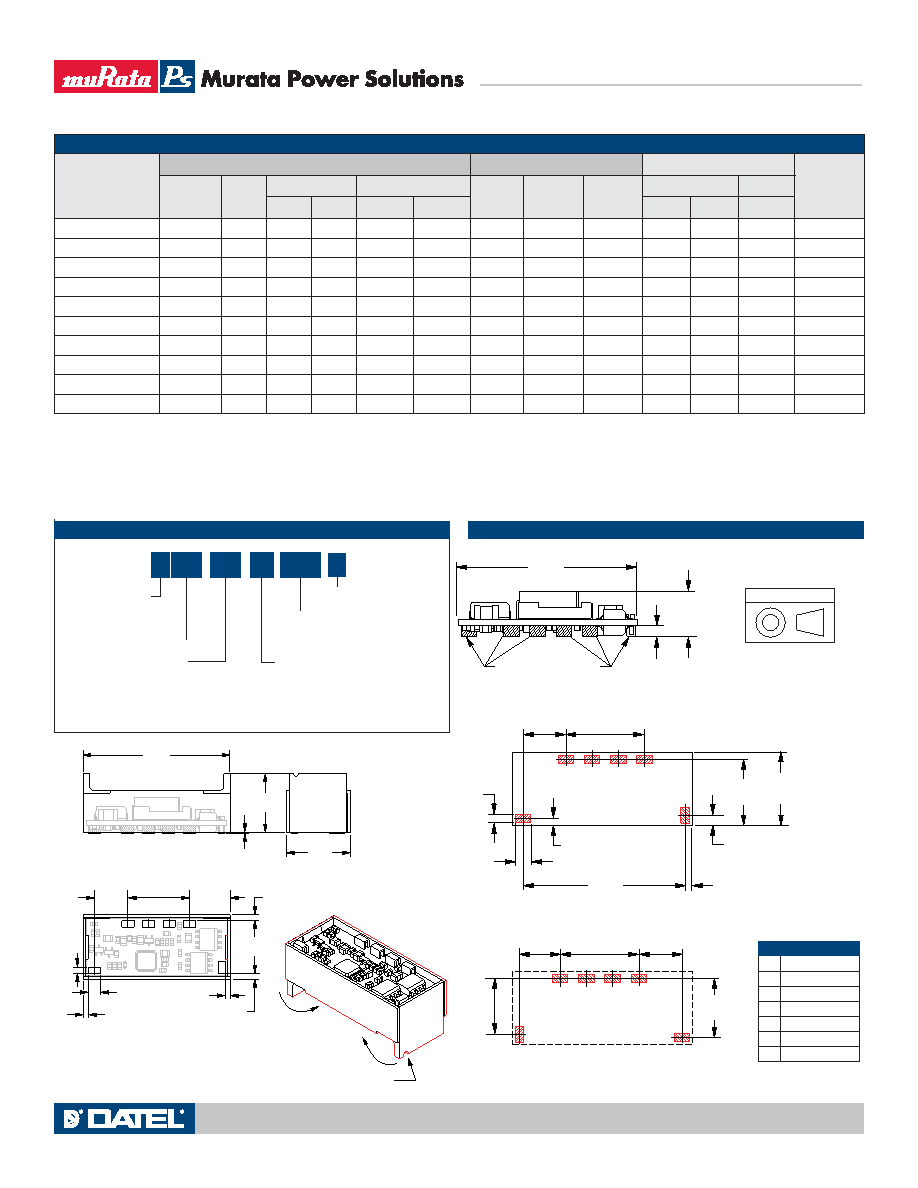
Pin
Function P63
1
On/Off Control
2
+Input
3
Common
4
+Output
5
VOUT Trim
6
+Sense
I/O Connections
Typical at TA = +25°C under nominal line voltage and full-load conditions, 200 lfm air ow for
extended operation, unless otherwise noted. All models are tested and specied with external
22F tantalum input and output capacitors. These capacitors are necessary to accommodate our
test equipment and may not be required to achieve specied performance in your applications.
See I/O Filtering and Noise Reduction.
Ripple/Noise (R/N) is tested/specied over a 20MHz bandwidth and may be reduced with external
ltering. See I/O Filtering and Noise Reduction for details.
These devices have no minimum-load requirements and will regulate under no-load conditions.
Regulation specications describe the output-voltage deviation as the line voltage or load is varied
from its nominal/midpoint value to either extreme.
Nominal line voltage, no-load/full-load conditions.
RoHS6 compliance does not claim EU RoHS exemption 7b–lead in solder.
Performance Specications and Ordering Guide
Case C45
0.34
(8.64)
0.53
(13.46)
0.48
(12.19)
0.430
(10.92)
0.405
(10.29)
0.085
(2.16)
1.30
(33.02)
SMT COPPER LEADS
COPLANAR 0.004
1.177
(29.90)
0.310
(7.87)
0.048
(1.22)
0.075
(1.91)
BOTTOM VIEW
RECOMMENDED PAD LAYOUT
0.05
(1.27)
0.062
(1.57)
TYP.
0.112
(2.84)
TYP.
0.570 (14.48)
3 EQ. SP. @
0.190 (4.83)
0.310
(7.87)
Recommended Pad Size: 0.15 x 0.10 (3.81 x 2.54)
0.297
(7.54)
0.570 (14.48)
3 EQ. SP. @
0.190 (4.83)
2
3
4
5
6
5
4
3
1
Maximum Rated Output
Current in Amps
Non-Isolated SMT
Output
Conguration:
L = Unipolar
Low Voltage
Nominal Output Voltage:
0.75, 1, 1.2, 1.5, 1.8, 2, 2.5, 3.3 or 5 Volts
Input Voltage Range:
D12 = 10 to 14 Volts
(12V nominal)
L SM
16
-
/
D12
-
1.8
1.36
( 34.54)
0.375
( 9.53)
0.112 T Y P.
( 2.84)
0.052
(1.32)
0.60
( 15.24)
0.049
( 1.24)
0.310
( 7.87)
0.010
( 0.254)
0.55
(13.97)
0.052
(1.32)
0.062
( 1.57)
0.047
(1.19)
0.570 ( 14.48)
3E Q . S P. @
0.190 ( 4.83)
2
345
6
1
NOTCH IN SHELL
INDICATES PIN ONE
CAUTION
PRESS TO REMOVE
THE HEAT SHIELD
AFTER THE SOLDER
PROCESS
NOTCH IN SHELL
INDICATES PIN ONE
LSM WITH REMOVABLE HEAT SHIELD
FOR HIGH TEMPERATURE SOLDER
BOTTOM VIEW
Note: Not all model number combinations
are available. Contact MPS.
-
RoHS6 hazardous substance
compliant*
C
* Contact Murata Power Solutions for
availability.
Part Number Structure
Mechanical Specifications
Third Angle Projection
Dimensions are in inches (mm shown for ref. only).
Components are shown for reference only.
Tolerances (unless otherwise specied):
.XX ± 0.02 (0.5)
.XXX ± 0.010 (0.25)
Angles ± 2
LSM-16A D12 Models
Non-Isolated, 13-80W SMT DC/DC Converters
MDC_LSM 16A D12 Models.A05 Page 2 of 12
Technical enquiries email: sales@murata-ps.com, tel: +1 508 339 3000
www.murata-ps.com
相關(guān)PDF資料 |
PDF描述 |
|---|---|
| LSM-1.8/16-D12-C | 1-OUTPUT DC-DC REG PWR SUPPLY MODULE |
| LSM-3.3/16-D12-C | 1-OUTPUT DC-DC REG PWR SUPPLY MODULE |
| LSM2-T/10-D12G-C | 1-OUTPUT 33 W DC-DC REG PWR SUPPLY MODULE |
| LSM2-T/6-W3N-C | 1-OUTPUT 19.8 W DC-DC REG PWR SUPPLY MODULE |
| LSM2-T/6-D12NG-C | 1-OUTPUT 19.8 W DC-DC REG PWR SUPPLY MODULE |
相關(guān)代理商/技術(shù)參數(shù) |
參數(shù)描述 |
|---|---|
| LSM271M2D---2225S | 制造商:Surge Components Inc 功能描述:CAP ALUM 270UF 200V ?20% 3000LHRS 22 X 25 - Bulk |
| LSM271M2E---2235S | 制造商:Surge Components Inc 功能描述:CAP ALUM 270UF 250V ?20% 3000LHRS 22 X 35 - Bulk |
| LSM271M2E---2525S | 制造商:Surge Components Inc 功能描述:CAP ALUM 270UF 250V ?20% 3000LHRS 25 X 25 - Bulk |
| LSM271M2G---2550S | 制造商:Surge Components Inc 功能描述:CAP ALUM 270UF 400V ?20% 3000LHRS 25 X 50 - Bulk |
| LSM271M2G---3040S | 制造商:Surge Components Inc 功能描述:CAP ALUM 270UF 400V ?20% 3000LHRS 30 X 40 - Bulk |
發(fā)布緊急采購,3分鐘左右您將得到回復(fù)。