- 您現(xiàn)在的位置:買賣IC網(wǎng) > PDF目錄358934 > LPC47N252 (SMSC Corporation) Advanced Notebook I/O Controller with On-Board FLASH PDF資料下載
參數(shù)資料
| 型號(hào): | LPC47N252 |
| 廠商: | SMSC Corporation |
| 英文描述: | Advanced Notebook I/O Controller with On-Board FLASH |
| 中文描述: | 先進(jìn)的筆記本電腦的I / O控制器板上閃存 |
| 文件頁數(shù): | 27/228頁 |
| 文件大?。?/td> | 1269K |
| 代理商: | LPC47N252 |
第1頁第2頁第3頁第4頁第5頁第6頁第7頁第8頁第9頁第10頁第11頁第12頁第13頁第14頁第15頁第16頁第17頁第18頁第19頁第20頁第21頁第22頁第23頁第24頁第25頁第26頁當(dāng)前第27頁第28頁第29頁第30頁第31頁第32頁第33頁第34頁第35頁第36頁第37頁第38頁第39頁第40頁第41頁第42頁第43頁第44頁第45頁第46頁第47頁第48頁第49頁第50頁第51頁第52頁第53頁第54頁第55頁第56頁第57頁第58頁第59頁第60頁第61頁第62頁第63頁第64頁第65頁第66頁第67頁第68頁第69頁第70頁第71頁第72頁第73頁第74頁第75頁第76頁第77頁第78頁第79頁第80頁第81頁第82頁第83頁第84頁第85頁第86頁第87頁第88頁第89頁第90頁第91頁第92頁第93頁第94頁第95頁第96頁第97頁第98頁第99頁第100頁第101頁第102頁第103頁第104頁第105頁第106頁第107頁第108頁第109頁第110頁第111頁第112頁第113頁第114頁第115頁第116頁第117頁第118頁第119頁第120頁第121頁第122頁第123頁第124頁第125頁第126頁第127頁第128頁第129頁第130頁第131頁第132頁第133頁第134頁第135頁第136頁第137頁第138頁第139頁第140頁第141頁第142頁第143頁第144頁第145頁第146頁第147頁第148頁第149頁第150頁第151頁第152頁第153頁第154頁第155頁第156頁第157頁第158頁第159頁第160頁第161頁第162頁第163頁第164頁第165頁第166頁第167頁第168頁第169頁第170頁第171頁第172頁第173頁第174頁第175頁第176頁第177頁第178頁第179頁第180頁第181頁第182頁第183頁第184頁第185頁第186頁第187頁第188頁第189頁第190頁第191頁第192頁第193頁第194頁第195頁第196頁第197頁第198頁第199頁第200頁第201頁第202頁第203頁第204頁第205頁第206頁第207頁第208頁第209頁第210頁第211頁第212頁第213頁第214頁第215頁第216頁第217頁第218頁第219頁第220頁第221頁第222頁第223頁第224頁第225頁第226頁第227頁第228頁
7
SMSC DS – LPC47M192
Page 27
Rev. 03/30/05
DATASHEET
FUNCTIONAL DESCRIPTION
The following sections describe the functional blocks located in the LPC47M192 (see FIGURE 1). All the
functional blocks are dedicated to the Super I/O portion of the chip, except for the Hardware Monitoring block.
The Hardware Monitoring block is maintained separately from the Super I/O components and is defined in
section 7.18
Hardware Monitoring Interface. It is powered by HVCC and all its registers are accessed through
an Internal Address register located in the Hardware Monitoring block (see section 10
Registers for Hardware
Monitoring Block). The various Super I/O components are described in the following sections and their registers
are implemented as typical Plug-and-Play components (see section 9
CONFIGURATION).
It should be noted that there are two main interfaces used to access the components of this chip. The LPC
interface is used to access the Super I/O registers and the SMBus is used to access the Hardware Monitoring
registers.
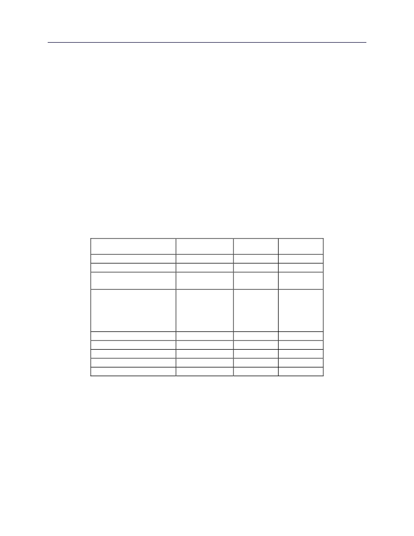
7.1 Super I/O Registers
The address map, shown below in Table 1 shows the addresses of the different blocks of the Super I/O
immediately after power up. The base addresses of the FDC, serial and parallel ports, PME register block,
Game port and configuration register block can be moved via the configuration registers. Some addresses are
used to access more than one register.
7.2 Host Processor Interface (LPC)
The host processor communicates with the LPC47M192 through a series of read/write registers via the LPC
interface. The port addresses for these registers are shown in Table 1. Register access is accomplished
through I/O cycles or DMA transfers. All registers are 8 bits wide.
Table 1 – Super I/O Block Addresses
ADDRESS
BLOCK NAME
LOGICAL
DEVICE
NOTES
Base+(0-5) and +(7)
Base+(0-7)
Base1+(0-7)
Base2+(0-7)
Base+(0-3)
Base+(0-7)
Base+(0-3), +(400-402)
Base+(0-7), +(400-402)
60, 64
Base + 0
Base + (0-5F)
Base + (0-1)
Base + (0-1)
Floppy Disk
Serial Port Com 1
Serial Port Com 2
0
4
5
Parallel Port
SPP
EPP
ECP
ECP+EPP+SPP
KYBD
Game Port
Runtime Registers
MPU-401
Configuration
3
7
9
A
B
Note 1
Note
: Refer to the configuration register descriptions for setting the base address.
Note 1
: Logical Device A is refered to as the Runtime Register block or PME Block and may be used
interchangeably throughout this document.
相關(guān)PDF資料 |
PDF描述 |
|---|---|
| LPC47N267 | 100 Pin LPC Notebook I/O with X-Bus Interface |
| LPC47M112 | ENHANCED SUPER I/O CONTROLLER WITH LPC INTERFACE |
| LPC47M112-MC | ENHANCED SUPER I/O CONTROLLER WITH LPC INTERFACE |
| LPC47M112-MW | ENHANCED SUPER I/O CONTROLLER WITH LPC INTERFACE |
| LPC47N252-SD | Advanced Notebook I/O Controller with On-Board FLASH |
相關(guān)代理商/技術(shù)參數(shù) |
參數(shù)描述 |
|---|---|
| LPC47N252-SD | 功能描述:輸入/輸出控制器接口集成電路 Advanced Notebook I/O Controller RoHS:否 制造商:Silicon Labs 產(chǎn)品: 輸入/輸出端數(shù)量: 工作電源電壓: 最大工作溫度:+ 85 C 最小工作溫度:- 40 C 安裝風(fēng)格:SMD/SMT 封裝 / 箱體:QFN-64 封裝:Tray |
| LPC47N252-SG | 功能描述:輸入/輸出控制器接口集成電路 Advanced Notebook I/O Controller RoHS:否 制造商:Silicon Labs 產(chǎn)品: 輸入/輸出端數(shù)量: 工作電源電壓: 最大工作溫度:+ 85 C 最小工作溫度:- 40 C 安裝風(fēng)格:SMD/SMT 封裝 / 箱體:QFN-64 封裝:Tray |
| LPC47N254-AAQ | 制造商:SMSC 功能描述: |
| LPC47N267 | 制造商:SMSC 制造商全稱:SMSC 功能描述:100 Pin LPC Super I/O with X-Bus Interface |
| LPC47N267_05 | 制造商:SMSC 制造商全稱:SMSC 功能描述:100 Pin LPC Super I/O with X-Bus Interface |
發(fā)布緊急采購,3分鐘左右您將得到回復(fù)。