- 您現(xiàn)在的位置:買賣IC網(wǎng) > PDF目錄385497 > LPC2921FBD100 (NXP SEMICONDUCTORS) ARM9 microcontroller with CAN, LIN, and USB PDF資料下載
參數(shù)資料
| 型號: | LPC2921FBD100 |
| 廠商: | NXP SEMICONDUCTORS |
| 元件分類: | 微控制器/微處理器 |
| 英文描述: | ARM9 microcontroller with CAN, LIN, and USB |
| 中文描述: | 32-BIT, FLASH, 125 MHz, RISC MICROCONTROLLER, PQFP100 |
| 封裝: | 14 X 14 MM, 1.40 MM HEIGHT, PLASTIC, MS-026, SOT407-1, LQFP-100 |
| 文件頁數(shù): | 35/84頁 |
| 文件大小: | 551K |
| 代理商: | LPC2921FBD100 |
第1頁第2頁第3頁第4頁第5頁第6頁第7頁第8頁第9頁第10頁第11頁第12頁第13頁第14頁第15頁第16頁第17頁第18頁第19頁第20頁第21頁第22頁第23頁第24頁第25頁第26頁第27頁第28頁第29頁第30頁第31頁第32頁第33頁第34頁當前第35頁第36頁第37頁第38頁第39頁第40頁第41頁第42頁第43頁第44頁第45頁第46頁第47頁第48頁第49頁第50頁第51頁第52頁第53頁第54頁第55頁第56頁第57頁第58頁第59頁第60頁第61頁第62頁第63頁第64頁第65頁第66頁第67頁第68頁第69頁第70頁第71頁第72頁第73頁第74頁第75頁第76頁第77頁第78頁第79頁第80頁第81頁第82頁第83頁第84頁
LPC2921_23_25_3
All information provided in this document is subject to legal disclaimers.
NXP B.V. 2010. All rights reserved.
Product data sheet
Rev. 03 — 14 April 2010
35 of 84
NXP Semiconductors
LPC2921/2923/2925
ARM9 microcontroller with CAN, LIN, and USB
A mechanism is provided to modify configuration of the ADC and control the moment at
which the updated configuration is transferred to the ADC domain.
The ADC clock is limited to 4.5 MHz maximum frequency and should always be lower
than or equal to the system clock frequency. To meet this constraint or to select the
desired lower sampling frequency, the clock generation unit provides a programmable
fractional system-clock divider dedicated to the ADC clock. Conversion rate is determined
by the ADC clock frequency divided by the number of resolution bits plus one. Accessing
ADC registers requires an enabled ADC clock, which is controllable via the clock
generation unit, see
Section 6.15.2
.
Each ADC has four start inputs. Note that start 0 and start 2 are captured in the system
clock domain while start 1 and start 3 are captured in the ADC domain. The start inputs
are connected at MSCSS level, see
Section 6.14
for details.
6.14.4.2
Pin description
The two ADC modules in the MSCSS have the pins described below. The ADCx input
pins are combined with other functions on the port pins of the LPC2921/2923/2925. The
VREFN and VREFP pins are common for both ADCs.
Table 20
shows the ADC pins.
Table 20.
Symbol
ADC1/2 IN[7:0]
Remark:
Note that the ADC1 and ADC2 accept an input voltage up to of 3.6 V (see
Table 31
) on the ADC1/2 IN pins. If the ADC is not used, the pins are 5 V tolerant.
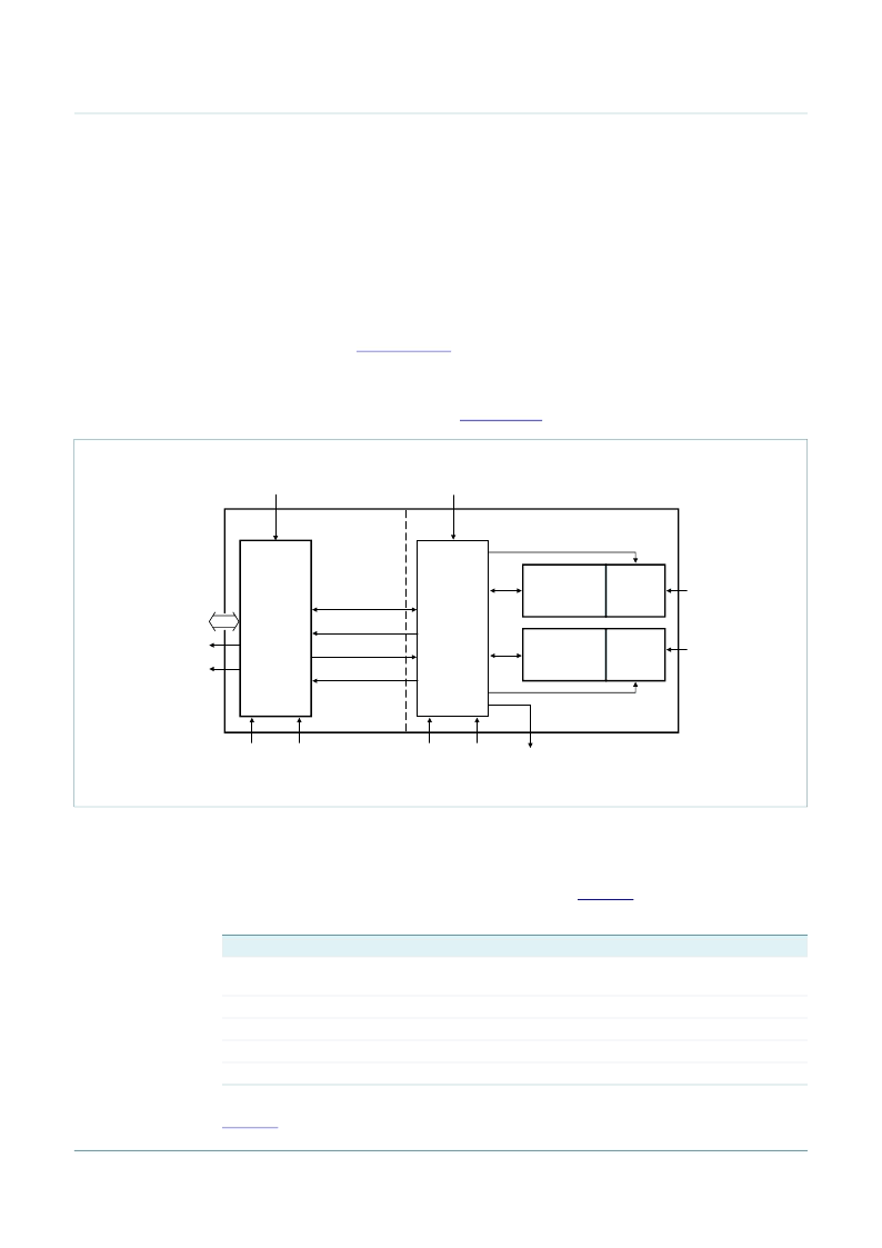
Fig 6.
ADC block diagram
002aad960
ADC
start 2
ADC
start 0
APB clock
(BASE_MSCSS_CLK)
ADC clock
(up to 4.5 MHz)
(BASE_ADC_CLK)
APB system bus
IRQ scan
IRQ compare
ADC2 IN[7:0]
ADC
start 1
ADC
start 3
sync_out
ADC DOMAIN
SYSTEM DOMAIN
ADC
CONTROL
ADC
REGISTERS
3.3 V
ADC2
3.3 V
ADC1
ANALOG
MUX
3.3 V IN
conversion data
update
configuration data
IRQ
ADC1 IN[7:0]
ANALOG
MUX
3.3 V IN
Analog to digital converter pins
Pin name
IN1/2[7:0]
Direction
IN
Description
analog input for 3.3 V ADC1/2, channel 7 to
channel 0
ADC external start-trigger input
ADC LOW reference level
ADC HIGH reference level
ADC1 and ADC2 3.3 V supply
ADC2_EXT_START
VREFN
VREFP
V
DDA(ADC3V3)
CAP1[2]
VREFN
VREFP
V
DDA(ADC3V3)
IN
IN
IN
IN
相關PDF資料 |
PDF描述 |
|---|---|
| LPC2923FBD100 | ARM9 microcontroller with CAN, LIN, and USB |
| LPC2925FBD100 | ARM9 microcontroller with CAN, LIN, and USB |
| LPC2926FBD144 | ARM9 microcontroller with CAN, LIN, and USB |
| LPC2927FBD144 | ARM9 microcontroller with CAN, LIN, and USB |
| LPC2929FBD144 | ARM9 microcontroller with CAN, LIN, and USB |
相關代理商/技術參數(shù) |
參數(shù)描述 |
|---|---|
| LPC2921FBD100,551 | 功能描述:ARM微控制器 - MCU IC ARM9 MCU FLASH 128KB RoHS:否 制造商:STMicroelectronics 核心:ARM Cortex M4F 處理器系列:STM32F373xx 數(shù)據(jù)總線寬度:32 bit 最大時鐘頻率:72 MHz 程序存儲器大小:256 KB 數(shù)據(jù) RAM 大小:32 KB 片上 ADC:Yes 工作電源電壓:1.65 V to 3.6 V, 2 V to 3.6 V, 2.2 V to 3.6 V 工作溫度范圍:- 40 C to + 85 C 封裝 / 箱體:LQFP-48 安裝風格:SMD/SMT |
| LPC2923 | 制造商:PHILIPS 制造商全稱:NXP Semiconductors 功能描述:ARM9 microcontroller with CAN, LIN, and USB |
| LPC2923FBD100 | 制造商:PHILIPS 制造商全稱:NXP Semiconductors 功能描述:ARM9 microcontroller with CAN, LIN, and USB device |
| LPC2923FBD100,551 | 功能描述:ARM微控制器 - MCU IC ARM9 MCU FLASH 256KB RoHS:否 制造商:STMicroelectronics 核心:ARM Cortex M4F 處理器系列:STM32F373xx 數(shù)據(jù)總線寬度:32 bit 最大時鐘頻率:72 MHz 程序存儲器大小:256 KB 數(shù)據(jù) RAM 大小:32 KB 片上 ADC:Yes 工作電源電壓:1.65 V to 3.6 V, 2 V to 3.6 V, 2.2 V to 3.6 V 工作溫度范圍:- 40 C to + 85 C 封裝 / 箱體:LQFP-48 安裝風格:SMD/SMT |
| LPC2925 | 制造商:PHILIPS 制造商全稱:NXP Semiconductors 功能描述:ARM9 microcontroller with CAN, LIN, and USB |
發(fā)布緊急采購,3分鐘左右您將得到回復。