- 您現在的位置:買賣IC網 > PDF目錄384605 > LP2997MR (NATIONAL SEMICONDUCTOR CORP) DDR-II Termination Regulator PDF資料下載
參數資料
| 型號: | LP2997MR |
| 廠商: | NATIONAL SEMICONDUCTOR CORP |
| 元件分類: | 通用總線功能 |
| 英文描述: | DDR-II Termination Regulator |
| 中文描述: | BUS TERMINATOR SUPPORT CIRCUIT, PDSO8 |
| 封裝: | PSOP-8 |
| 文件頁數: | 7/12頁 |
| 文件大小: | 233K |
| 代理商: | LP2997MR |
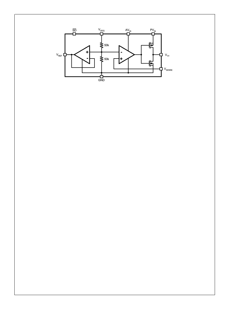
Block Diagram
20109405
Description
The LP2997 is a linear bus termination regulator designed to
meet the JEDEC requirements of SSTL-18. The output, V
TT
is capable of sinking and sourcing current while regulating
the output voltage equal to VDDQ / 2. The output stage has
been designed to maintain excellent load regulation while
preventing shoot through. The LP2997 also incorporates two
distinct power rails that separates the analog circuitry from
the power output stage. This allows a split rail approach to
be utilized to decrease internal power dissipation. It also
permits the LP2997 to provide a termination solution for the
next generation of DDR-SDRAM memory (DDRII).
Pin Descriptions
AVIN AND PVIN
AVIN and PVIN are the input supply pins for the LP2997.
AVIN is used to supply all the internal control circuitry. PVIN,
however, is used exclusively to provide the rail voltage for
the output stage used to create V
. These pins have the
capability to work off separate supplies, under the condition
that AVIN is always greater than or equal to PVIN. For
SSTL-18 applications, it is recommended to connect PVIN to
the 1.8V rail used for the memory core and AVIN to a rail
within its operating range of 2.2V to 5.5V (typically a 2.5V
supply). PVIN should always be used with either a 1.8V or
2.5V rail. This prevents the thermal limit from tripping be-
cause of excessive internal power dissipation. If the junction
temperature exceeds the thermal shutdown than the part will
enter a shutdown state identical to the manual shutdown
where V
TT
is tri-stated and V
REF
remains active. A lower rail
such as 1.5V can be used but it will reduce the maximum
output current, therefore it is not recommended for most
termination schemes.
VDDQ
VDDQ is the input used to create the internal reference
voltage for regulating V
. The reference voltage is gener-
ated from a resistor divider of two internal 50k
resistors.
This guarantees that V
will track VDDQ / 2 precisely. The
optimal implementation of VDDQ is as a remote sense. This
can be achieved by connecting VDDQ directly to the 1.8V
rail at the DIMM instead of PVIN. This ensures that the
reference voltage tracks the DDR memory rails precisely
without a large voltage drop from the power lines. For
SSTL-18 applications VDDQ will be a 1.8V signal, which will
create a 0.9V termination voltage at V
TT
(See Electrical
Characteristics Table for exact values of V
TT
over tempera-
ture).
V
SENSE
The purpose of the sense pin is to provide improved remote
load regulation. In most motherboard applications the termi-
nation resistors will connect to V
TT
in a long plane. If the
output voltage was regulated only at the output of the
LP2997 then the long trace will cause a significant IR drop
resulting in a termination voltage lower at one end of the bus
than the other. The V
pin can be used to improve this
performance, by connecting it to the middle of the bus. This
will provide a better distribution across the entire termination
bus. If remote load regulation is not used then the V
pin must still be connected to V
. Care should be taken
when a long V
trace is implemented in close proximity
to the memory. Noise pickup in the V
SENSE
trace can cause
problems with precise regulation of V
TT
ramic capacitor placed next to the V
pin can help filter
any high frequency signals and preventing errors.
SHUTDOWN
The LP2997 contains an active low shutdown pin that can be
used for suspend to RAM functionality. In this condition the
V
output will tri-state while the V
output remains active
providing a constant reference signal for the memory and
chipset. During shutdown V
TT
should not be exposed to
voltages that exceed PVIN. With the shutdown pin asserted
low the quiescent current of the LP2997 will drop, however,
VDDQ will always maintain its constant impedance of 100k
for generating the internal reference. Therefore, to calculate
the total power loss in shutdown both currents need to be
considered. For more information refer to the Thermal Dis-
sipation section. The shutdown pin also has an internal
pull-up current; therefore, to turn the part on the shutdown
pin can either be connected to AVIN or left open
V
REF
V
provides the buffered output of the internal reference
voltage VDDQ / 2. This output should be used to provide the
reference voltage for the Northbridge chipset and memory.
Since these inputs are typically an extremely high imped-
ance, there should be little current drawn from V
. For
improved performance, an output bypass capacitor can be
used, located close to the pin, to help with noise. A ceramic
capacitor in the range of 0.1 μF to 0.01 μF is recommended.
L
www.national.com
7
相關PDF資料 |
PDF描述 |
|---|---|
| LP2997MX | DDR-II Termination Regulator |
| LP2997 | Hex Inverters 14-TSSOP -40 to 85 |
| LP3950 | Color LED Driver with Audio Synchronizer |
| LP3950SL | Color LED Driver with Audio Synchronizer |
| LP3950SLX | Color LED Driver with Audio Synchronizer |
相關代理商/技術參數 |
參數描述 |
|---|---|
| LP2997MR NOPB | 制造商:Texas Instruments 功能描述: |
| LP2997MR/NOPB | 功能描述:線性穩(wěn)壓器 - 標準 DDR Termination Reg RoHS:否 制造商:STMicroelectronics 輸出類型: 極性: 輸出電壓:1.8 V 輸出電流:150 mA 負載調節(jié): 最大輸入電壓:5.5 V 線路調整率: 最大工作溫度:+ 125 C 安裝風格:SMD/SMT 封裝 / 箱體:SOT-323-5L |
| LP2997MRX | 功能描述:線性穩(wěn)壓器 - 標準 RoHS:否 制造商:STMicroelectronics 輸出類型: 極性: 輸出電壓:1.8 V 輸出電流:150 mA 負載調節(jié): 最大輸入電壓:5.5 V 線路調整率: 最大工作溫度:+ 125 C 安裝風格:SMD/SMT 封裝 / 箱體:SOT-323-5L |
| LP2997MRX/NOPB | 功能描述:線性穩(wěn)壓器 - 標準 RoHS:否 制造商:STMicroelectronics 輸出類型: 極性: 輸出電壓:1.8 V 輸出電流:150 mA 負載調節(jié): 最大輸入電壓:5.5 V 線路調整率: 最大工作溫度:+ 125 C 安裝風格:SMD/SMT 封裝 / 箱體:SOT-323-5L |
| LP2997MX | 功能描述:線性穩(wěn)壓器 - 標準 RoHS:否 制造商:STMicroelectronics 輸出類型: 極性: 輸出電壓:1.8 V 輸出電流:150 mA 負載調節(jié): 最大輸入電壓:5.5 V 線路調整率: 最大工作溫度:+ 125 C 安裝風格:SMD/SMT 封裝 / 箱體:SOT-323-5L |
發(fā)布緊急采購,3分鐘左右您將得到回復。