- 您現(xiàn)在的位置:買(mǎi)賣(mài)IC網(wǎng) > PDF目錄384605 > LP2997M (NATIONAL SEMICONDUCTOR CORP) DDR-II Termination Regulator PDF資料下載
參數(shù)資料
| 型號(hào): | LP2997M |
| 廠商: | NATIONAL SEMICONDUCTOR CORP |
| 元件分類(lèi): | 通用總線功能 |
| 英文描述: | DDR-II Termination Regulator |
| 中文描述: | BUS TERMINATOR SUPPORT CIRCUIT, PDSO8 |
| 封裝: | SOP-8 |
| 文件頁(yè)數(shù): | 10/12頁(yè) |
| 文件大小: | 233K |
| 代理商: | LP2997M |
Typical Application Circuits
Several different application circuits have been shown to
illustrate some of the options that are possible in configuring
the LP2997. Graphs of the individual circuit performance can
be found in the
Typical Performance Characteristics
section
in the beginning of the datasheet. These curves illustrate
how the maximum output current is affected by changes in
AVIN and PVIN.
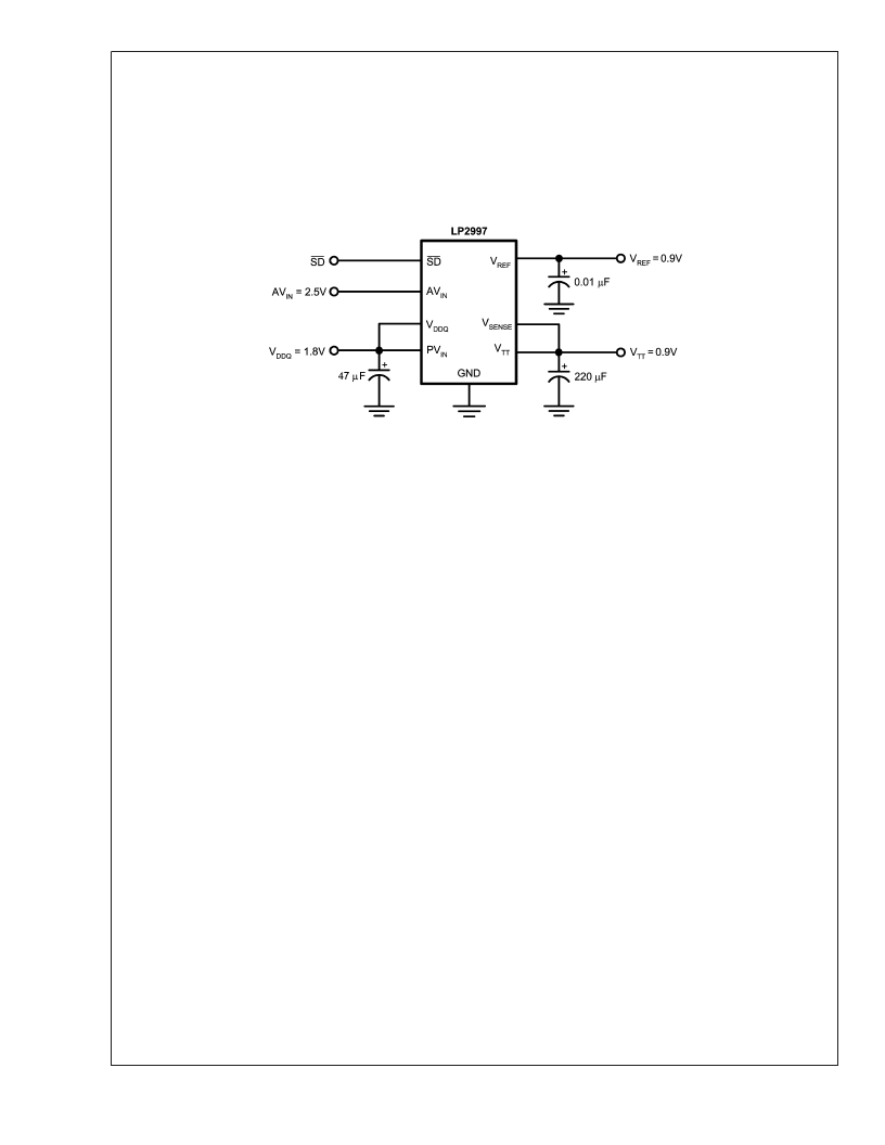
Figure 2
shows the recommended circuit configuration for
DDR-II applications. The output stage is connected to the
1.8V rail and the AVIN pin can be connected to either a 2.5V,
3.3V or 5V rail.
This circuit permits termination in a minimum amount of
board space and component count. Capacitor selection can
be varied depending on the number of lines terminated and
the maximum load transient. However, with motherboards
and other applications where V
is distributed across a long
plane it is advisable to use multiple bulk capacitors and
addition to high frequency decoupling. The bulk output ca-
pacitors should be situated at both ends of the V
plane for
optimal placement. Large aluminum electrolytic capacitors
are used for their low ESR and low cost.
PCB Layout Considerations
1.
The input capacitor for the power rail should be placed
as close as possible to the PVIN pin.
2.
V
SENSE
should be connected to the V
TT
termination bus
at the point where regulation is required. For mother-
board applications an ideal location would be at the
center of the termination bus.
3.
V
can be connected remotely to the V
rail input
at either the DIMM or the Chipset. This provides the
most accurate point for creating the reference voltage.
For improved thermal performance excessive top side
copper should be used to dissipate heat from the pack-
age. Numerous vias from the ground connection to the
internal ground plane will help. Additionally these can be
located underneath the package if manufacturing stan-
dards permit.
Care should be taken when routing the V
trace to
avoid noise pickup from switching I/O signals. A 0.1uF
ceramic capacitor located close to the
can also be
used to filter any unwanted high frequency signal. This
can be an issue especially if long
SENSE
traces are used.
V
REF
should be bypassed with a 0.01 μF or 0.1 μF
ceramic capacitor for improved performance. This ca-
pacitor should be located as close as possible to the
V
REF
pin.
4.
5.
6.
20109413
FIGURE 2. Recommended DDR-II Termination
L
www.national.com
10
相關(guān)PDF資料 |
PDF描述 |
|---|---|
| LP2997MR | DDR-II Termination Regulator |
| LP2997MX | DDR-II Termination Regulator |
| LP2997 | Hex Inverters 14-TSSOP -40 to 85 |
| LP3950 | Color LED Driver with Audio Synchronizer |
| LP3950SL | Color LED Driver with Audio Synchronizer |
相關(guān)代理商/技術(shù)參數(shù) |
參數(shù)描述 |
|---|---|
| LP2997M/NOPB | 功能描述:線性穩(wěn)壓器 - 標(biāo)準(zhǔn) DDR Termination Reg RoHS:否 制造商:STMicroelectronics 輸出類(lèi)型: 極性: 輸出電壓:1.8 V 輸出電流:150 mA 負(fù)載調(diào)節(jié): 最大輸入電壓:5.5 V 線路調(diào)整率: 最大工作溫度:+ 125 C 安裝風(fēng)格:SMD/SMT 封裝 / 箱體:SOT-323-5L |
| LP2997MR | 功能描述:線性穩(wěn)壓器 - 標(biāo)準(zhǔn) RoHS:否 制造商:STMicroelectronics 輸出類(lèi)型: 極性: 輸出電壓:1.8 V 輸出電流:150 mA 負(fù)載調(diào)節(jié): 最大輸入電壓:5.5 V 線路調(diào)整率: 最大工作溫度:+ 125 C 安裝風(fēng)格:SMD/SMT 封裝 / 箱體:SOT-323-5L |
| LP2997MR NOPB | 制造商:Texas Instruments 功能描述: |
| LP2997MR/NOPB | 功能描述:線性穩(wěn)壓器 - 標(biāo)準(zhǔn) DDR Termination Reg RoHS:否 制造商:STMicroelectronics 輸出類(lèi)型: 極性: 輸出電壓:1.8 V 輸出電流:150 mA 負(fù)載調(diào)節(jié): 最大輸入電壓:5.5 V 線路調(diào)整率: 最大工作溫度:+ 125 C 安裝風(fēng)格:SMD/SMT 封裝 / 箱體:SOT-323-5L |
| LP2997MRX | 功能描述:線性穩(wěn)壓器 - 標(biāo)準(zhǔn) RoHS:否 制造商:STMicroelectronics 輸出類(lèi)型: 極性: 輸出電壓:1.8 V 輸出電流:150 mA 負(fù)載調(diào)節(jié): 最大輸入電壓:5.5 V 線路調(diào)整率: 最大工作溫度:+ 125 C 安裝風(fēng)格:SMD/SMT 封裝 / 箱體:SOT-323-5L |
發(fā)布緊急采購(gòu),3分鐘左右您將得到回復(fù)。