- 您現(xiàn)在的位置:買賣IC網(wǎng) > PDF目錄361044 > LMX2531 (National Semiconductor Corporation) PLLatinum High Performance Frequency Synthesizer System with Integrated VCO PDF資料下載
參數(shù)資料
| 型號: | LMX2531 |
| 廠商: | National Semiconductor Corporation |
| 英文描述: | PLLatinum High Performance Frequency Synthesizer System with Integrated VCO |
| 中文描述: | PLLatinum高性能頻率合成器系統(tǒng)的集成VCO |
| 文件頁數(shù): | 3/25頁 |
| 文件大小: | 589K |
| 代理商: | LMX2531 |
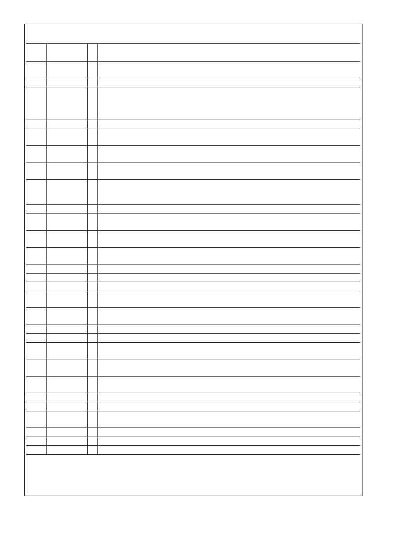
Pin Descriptions
Pin
Number
Pin Name
I/O Description
1
VccDIG
-
Power Supply for digital LDO circuitry. Input may range from 2.8 - 3.2 V. Bypass capacitors should be
placed as close as possible to this pin and ground.
Ground
3
GND
-
2,4,5,7,
12,
13,
29, 35
6
NC
-
No Connect.
VregBUF
-
Internally regulated voltage for the VCO buffer circuitry. Connect to ground with a capacitor.
MICROWIRE serial data input. High impedance CMOS input. This pin must not exceed 2.75V. Data is
clocked in MSB first. The last bits clocked in form the control or register select bits.
MICROWIRE clock input. High impedance CMOS input. This pin must not exceed 2.75V. Data is
clocked into the shift register on the rising edge.
MICROWIRE Latch Enable input. High impedance CMOS input. This pin must not exceed 2.75V.
Data stored in the shift register is loaded into the selected latch register when LE goes HIGH.
Chip Enable Input. High impedance CMOS input. This pin must not exceed 2.75V. When CE is
brought high the LMX2531 is powered up corresponding to the internal power control bits. It is
necessary to reprogram the R0 register to get the part to re-lock.
No Connect. Do NOT ground.
Power Supply for VCO regulator circuitry. Input may range from 2.8 - 3.2 V. Bypass capacitors should
be placed as close as possible to this pin and ground.
Internally regulated voltage for VCO circuitry. Not intended to drive an external load. Connect to
ground with a capacitor and some series resistance.
Internal reference voltage for VCO LDO. Not intended to drive an external load. Connect to ground
with a capacitor.
Ground for the VCO circuitry.
Ground for the RF Output Buffer circuitry.
O Buffered RF Output for the VCO.
Power Supply for the VCO Buffer circuitry. Input may range from 2.8 - 3.2 V. Bypass capacitors
should be placed as close as possible to this pin and ground.
Tuning voltage input for the VCO. For connection to the CPout Pin through an external passive loop
filter.
O Charge pump output for PLL. For connection to Vtune through an external passive loop filter.
O An open drain NMOS output which is used for FastLock or a general purpose output.
Internally regulated voltage for PLL charge pump. Not intended to drive an external load. Connect to
ground with a capacitor.
Power Supply for the PLL. Input may range from 2.8 - 3.2 V. Bypass capacitors should be placed as
close as possible to this pin and ground.
Internally regulated voltage for RF digital circuitry. Not intended to drive an external load. Connect to
ground with a capacitor.
O Multiplexed CMOS output. Typically used to monitor PLL lock condition.
I
Oscillator input. The oscillator can be placed in either single-ended or differential mode of operation.
Oscillator complimentary input. When a single ended source is used, then a bypass capacitor should
be placed as close as possible to this pin and be connected to ground.
O This pin if for test purposes and should be grounded for normal operation.
-
Ground
-
Internally regulated voltage for LDO digital circuitry.
8
DATA
I
9
CLK
I
10
LE
I
11
CE
I
14, 15
NC
-
16
VccVCO
-
17
VregVCO
-
18
VrefVCO
-
19
20
21
GND
GND
Fout
-
-
22
VccBUF
-
23
Vtune
I
24
25
CPout
FLout
26
VregPLL1
-
27
VccPLL
-
28
VregPLL2
-
30
31
Ftest/LD
OSCin
32
OSCin*
I
33
34
36
Test
GND
VregDIG
L
www.national.com
3
相關(guān)PDF資料 |
PDF描述 |
|---|---|
| LMX2531LQ1650E | PLLatinum High Performance Frequency Synthesizer System with Integrated VCO |
| LMX2531LQ1778E | PLLatinum High Performance Frequency Synthesizer System with Integrated VCO |
| LMX2531LQ2080E | PLLatinum High Performance Frequency Synthesizer System with Integrated VCO |
| LMX2531LQ2265E | OPTOCOUPLER, TRANSISTOR O/P; Channels, No. of:1; Voltage, isolation:5300V; Output type:Transistor; Current, input:60mA; Voltage, output max:55V; Case style:DIL; Temperature, operating range:-55(degree C) to ?(degree C); Approval RoHS Compliant: Yes |
| LMX2531LQ2570E | PLLatinum High Performance Frequency Synthesizer System with Integrated VCO |
相關(guān)代理商/技術(shù)參數(shù) |
參數(shù)描述 |
|---|---|
| LMX2531_07 | 制造商:NSC 制造商全稱:National Semiconductor 功能描述:High Performance Frequency Synthesizer System with Integrated VCO |
| LMX25311146EVAL | 功能描述:時鐘和定時器開發(fā)工具 LMX2531LQ1146 EVAL BOARD RoHS:否 制造商:Texas Instruments 產(chǎn)品:Evaluation Modules 類型:Clock Conditioners 工具用于評估:LMK04100B 頻率:122.8 MHz 工作電源電壓:3.3 V |
| LMX25311146EVAL/NOPB | 功能描述:射頻開發(fā)工具 LMX25311146 EVAL MOD RoHS:否 制造商:Taiyo Yuden 產(chǎn)品:Wireless Modules 類型:Wireless Audio 工具用于評估:WYSAAVDX7 頻率: 工作電源電壓:3.4 V to 5.5 V |
| LMX25311226EVAL | 功能描述:時鐘和定時器開發(fā)工具 LMX2531LQ1226 EVAL BOARD RoHS:否 制造商:Texas Instruments 產(chǎn)品:Evaluation Modules 類型:Clock Conditioners 工具用于評估:LMK04100B 頻率:122.8 MHz 工作電源電壓:3.3 V |
| LMX25311226EVAL/NOPB | 功能描述:射頻開發(fā)工具 LMX25311226 EVAL MOD RoHS:否 制造商:Taiyo Yuden 產(chǎn)品:Wireless Modules 類型:Wireless Audio 工具用于評估:WYSAAVDX7 頻率: 工作電源電壓:3.4 V to 5.5 V |
發(fā)布緊急采購,3分鐘左右您將得到回復(fù)。