- 您現(xiàn)在的位置:買賣IC網(wǎng) > PDF目錄358881 > LMH6704MA (NATIONAL SEMICONDUCTOR CORP) 650 MHz Progammable Gain Buffer with Disable PDF資料下載
參數(shù)資料
| 型號: | LMH6704MA |
| 廠商: | NATIONAL SEMICONDUCTOR CORP |
| 元件分類: | 音頻/視頻放大 |
| 英文描述: | 650 MHz Progammable Gain Buffer with Disable |
| 中文描述: | 1 CHANNEL, VIDEO AMPLIFIER, PDSO8 |
| 封裝: | SOIC-8 |
| 文件頁數(shù): | 9/12頁 |
| 文件大小: | 774K |
| 代理商: | LMH6704MA |
Application Section
(Continued)
Disabled, the LMH6704 inputs and output become high im-
pedances. While disabled the LMH6704 quiescent current is
approximately 250 μA. Because of the pull up resistor on the
disable circuit, the I
CC
and I
EE
currents (positive and nega-
tive supply currents respectively) are not balanced in the
disabled state. The positive supply current (I
) is approxi-
mately 350 μA while the negative supply current (I
) is only
250 μA. The remaining I
EE
current of 100 μA flows through
the disable pin.
The disable function can be used to create analog switches
or multiplexers. Implement a single analog switch with one
LMH6704 positioned between an input and output. Create
an analog multiplexer with several LMH6704’s. Use the cir-
cuit shown in for multiplexer applications because there is no
RG to shunt signals to ground.
EVALUATION BOARDS
National Semiconductor provides the following evaluation
boards as a guide for high frequency layout and as an aid in
device testing and characterization. Many of the datasheet
plots were measured with these boards.
Device
Package
Evaluation Board
Part Number
CLC730227
CLC730216
LMH6704MA
LMH6704MF
SOIC-8
SOT23-6
An evaluation board is shipped upon request when a sample
order is placed with National Semiconductor.
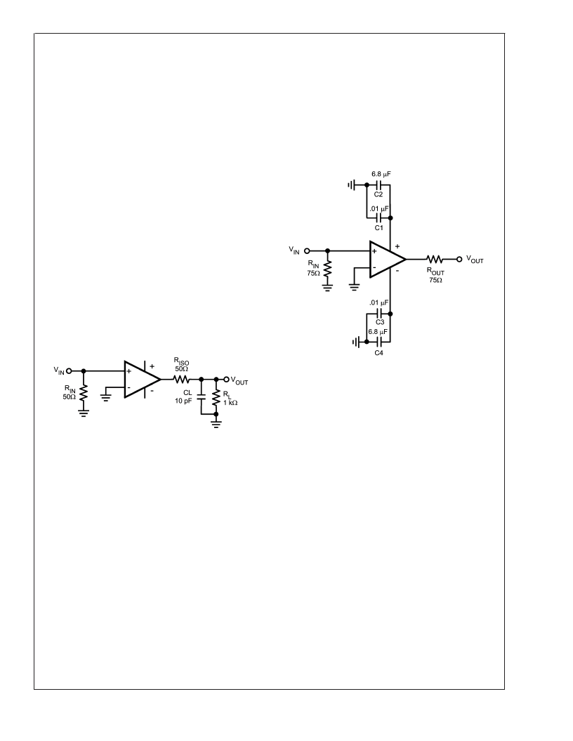
DRIVING CAPACITIVE LOADS
Capacitive output loading applications will benefit from the
use of a series output resistor R
ISO
.
Figure 7
shows the use
of a series output resistor, R
ISO
, to stabilize the amplifier
output under capacitive loading. Capacitive loads of 5 to 120
pF are the most critical, causing ringing, frequency response
peaking and possible oscillation. The chart “Suggested R
vs. Cap Load” gives a recommended value for selecting a
series output resistor for mitigating capacitive loads. The
values suggested in the charts are selected for .5 dB or less
of peaking in the frequency response. This gives a good
compromise between settling time and bandwidth. For appli-
cations where maximum frequency response is needed and
some peaking is tolerable, the value of R
ISO
can be reduced
slightly from the recommended values.
LAYOUT CONSIDERATIONS
Whenever questions about layout arise, use the evaluation
board as a guide. The CLC730216 is the evaluation board
supplied with samples of the LMH6704. To reduce parasitic
capacitances ground and power planes should be removed
near the input and output pins. For long signal paths con-
trolled impedance lines should be used, along with imped-
ance matching elements at both ends. Bypass capacitors
should be placed as close to the device as possible. Bypass
capacitors from each rail to ground are applied in pairs. The
larger electrolytic bypass capacitors can be located farther
from the device, the smaller ceramic capacitors should be
placed as close to the device as possible. In
Figure 1
,
Figure
2
, and
Figure 3
C
SS
is optional, but is recommended for best
second order harmonic distortion. Another option to using
C
SS
is to use pairs of 0.01 μF and 0.1 μF ceramic capacitors
for each supply bypass.
VIDEO PERFORMANCE
The LMH6704 has been designed to provide excellent per-
formance with production quality video signals in a wide
variety of formats such as HDTV and High Resolution VGA.
NTSC and PAL performance is nearly flawless with DG of
0.02% and DP of 0.02. Best performance will be obtained
with back terminated loads. The back termination reduces
reflections from the transmission line and effectively masks
transmission line and other parasitic capacitances from the
amplifier output stage.
Figure 8
shows a typical configuration
for driving a 75
Cable. The amplifier is configured for a gain
of two to make up for the 6 dB of loss in R
OUT
.
POWER DISSIPATION
Follow these steps to determine the Maximum power dissi-
pation for the LMH6704:
1.
Calculate the quiescent (no-load) power:
P
AMP
= I
CC*
(V
S
), where V
S
= V
+
- V
2.
Calculate the RMS power dissipated in the output stage:
P
D
(rms) = rms ((V
S
- V
OUT
)*I
OUT
), where V
OUT
and I
OUT
are the voltage and current across the external load and
V
S
is the total supply current
3.
Calculate the total RMS power: P
T
= P
AMP
+P
D
The maximum power that the LMH6704, package can dissi-
pate at a given temperature can be derived with the following
equation:
20103606
FIGURE 7. Decoupling Capacitive Loads
20103608
FIGURE 8. Typical Video Application
L
www.national.com
9
相關(guān)PDF資料 |
PDF描述 |
|---|---|
| LMH6704MAX | 650 MHz Progammable Gain Buffer with Disable |
| LMH6704MF | 650 MHz Progammable Gain Buffer with Disable |
| LMH6704MFX | 650 MHz Progammable Gain Buffer with Disable |
| LMH6704 | 650 MHz Progammable Gain Buffer with Disable |
| LMH6718MA | 5V High-Speed RS-232 Transceivers with 0.1uF Capacitors |
相關(guān)代理商/技術(shù)參數(shù) |
參數(shù)描述 |
|---|---|
| LMH6704MA/NOPB | 功能描述:特殊用途放大器 RoHS:否 制造商:Texas Instruments 通道數(shù)量:Single 共模抑制比(最小值): 輸入補(bǔ)償電壓: 工作電源電壓:3 V to 5.5 V 電源電流:5 mA 最大功率耗散: 最大工作溫度:+ 70 C 最小工作溫度:- 40 C 安裝風(fēng)格:SMD/SMT 封裝 / 箱體:QFN-20 封裝:Reel |
| LMH6704MAX | 功能描述:特殊用途放大器 RoHS:否 制造商:Texas Instruments 通道數(shù)量:Single 共模抑制比(最小值): 輸入補(bǔ)償電壓: 工作電源電壓:3 V to 5.5 V 電源電流:5 mA 最大功率耗散: 最大工作溫度:+ 70 C 最小工作溫度:- 40 C 安裝風(fēng)格:SMD/SMT 封裝 / 箱體:QFN-20 封裝:Reel |
| LMH6704MAX/NOPB | 功能描述:特殊用途放大器 RoHS:否 制造商:Texas Instruments 通道數(shù)量:Single 共模抑制比(最小值): 輸入補(bǔ)償電壓: 工作電源電壓:3 V to 5.5 V 電源電流:5 mA 最大功率耗散: 最大工作溫度:+ 70 C 最小工作溫度:- 40 C 安裝風(fēng)格:SMD/SMT 封裝 / 箱體:QFN-20 封裝:Reel |
| LMH6704MF | 功能描述:特殊用途放大器 RoHS:否 制造商:Texas Instruments 通道數(shù)量:Single 共模抑制比(最小值): 輸入補(bǔ)償電壓: 工作電源電壓:3 V to 5.5 V 電源電流:5 mA 最大功率耗散: 最大工作溫度:+ 70 C 最小工作溫度:- 40 C 安裝風(fēng)格:SMD/SMT 封裝 / 箱體:QFN-20 封裝:Reel |
| LMH6704MF/NOPB | 功能描述:特殊用途放大器 650MHz Selectable Gain Buffer RoHS:否 制造商:Texas Instruments 通道數(shù)量:Single 共模抑制比(最小值): 輸入補(bǔ)償電壓: 工作電源電壓:3 V to 5.5 V 電源電流:5 mA 最大功率耗散: 最大工作溫度:+ 70 C 最小工作溫度:- 40 C 安裝風(fēng)格:SMD/SMT 封裝 / 箱體:QFN-20 封裝:Reel |
發(fā)布緊急采購,3分鐘左右您將得到回復(fù)。