- 您現(xiàn)在的位置:買(mǎi)賣(mài)IC網(wǎng) > PDF目錄384601 > LM8342SDX (NATIONAL SEMICONDUCTOR CORP) Programmable TFT VCOM Calibrator with Non-Volatile PDF資料下載
參數(shù)資料
| 型號(hào): | LM8342SDX |
| 廠商: | NATIONAL SEMICONDUCTOR CORP |
| 元件分類(lèi): | 消費(fèi)家電 |
| 英文描述: | Programmable TFT VCOM Calibrator with Non-Volatile |
| 中文描述: | SPECIALTY CONSUMER CIRCUIT, DSO10 |
| 封裝: | LLP-10 |
| 文件頁(yè)數(shù): | 15/16頁(yè) |
| 文件大?。?/td> | 951K |
| 代理商: | LM8342SDX |
第1頁(yè)第2頁(yè)第3頁(yè)第4頁(yè)第5頁(yè)第6頁(yè)第7頁(yè)第8頁(yè)第9頁(yè)第10頁(yè)第11頁(yè)第12頁(yè)第13頁(yè)第14頁(yè)當(dāng)前第15頁(yè)第16頁(yè)
Typical Application
(Continued)
TABLE 4. Overview Resistor Values for Different R
SET
Settings at AV
DD
= 15V
AV
DD
= 15V (V
COM
Level = 7.5 V)
R
SET
= 10 k
V
COM
(V)
(
)
(
)
±
0.5
25k
28.6k
±
1
47.1k
61.5k
±
1.5
66.7k
100k
±
2
84.2k
146k
±
2.5
100k
200k
±
3
114k
267k
R
SET
= 45 k
V
COM
(V)
±
0.5
±
1
±
1.5
±
2
±
2.5
±
3
R1
R2
R1
(
)
113k
212k
300k
379k
450k
514k
R2
(
)
129k
277k
450k
655k
900k
1.2M
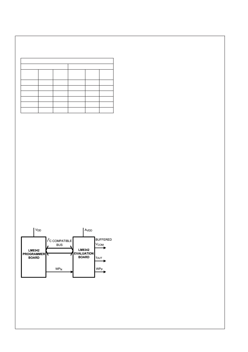
EVALUATION SYSTEM
For the LM8342 a complete evaluation system is available,
including two boards.
Figure 10
gives a schematic represen-
tation.
LM8342 Evaluation Board
This board demonstrates the functionality of the LM8342
using the I
2
C compatible interface for communication.
The LM8342 can easily be demonstrated in 2 applica-
tions:
— Programmable current sink
— Programmable V
COM
level driver
LM8342 Programmer Board
This test board has dedicated functionality for communi-
cating with the LM8342, using the I
2
C compatible inter-
face. This board can operate in two different modes:
—
Write mode:
The digitized value of a potentiometer
setting is written to the LM8342. The user can select
on the programmer board to write the data to the
register or to store the data in the EEPROM.
—
Read mode:
The board reads the stored values from
the LM8342’s EEPROM and presents this data onto a
3-digit display.
LAYOUT RECOMMENDATIONS
A proper layout is necessary for optimum performance of the
LM8342. A low impedance and proper ground plane (free of
disturbances) is recommended, since a current of up to 10
mA can flow with HF contents during programming. The
traces from the GND pin to the ground plane should be as
short as possible. It is recommended to place decoupling
capacitors close to the V
and AV
pins. Connections of
these decoupling capacitors to the ground plane should be
short.
As SET is a sensitive input, crosstalk to that pin should be
prevented. Special care should be taken when routing the
interface connections. The signals on the serial interface can
be more than 60 dB larger than the equivalent LSB at the
SET input pin. Crosstalk between the interface bus and R
SET
results in disturbance of the output current I
OUT
of the
LM8342.
For applications requiring a low output current (using high
values for R
in combination with low DAC settings) spe-
cial attention should be paid to the parasitic capacitance
(C
) parallel to R
. For C
larger than tens of pF, a
small (
<
1 LSB) unwanted ripple at the output current might
be obtained. It is recommended to place the R
resistor
close to the LM8342, in combination with a good board
layout to reduce this parasitic capacitance.
20139232
FIGURE 10. LM8342 Evaluation System
L
www.national.com
15
相關(guān)PDF資料 |
PDF描述 |
|---|---|
| LM883E | 3-Terminal Adjustable Regulator |
| LM883K | 3-Terminal Adjustable Regulator |
| LM883HVKSTL | 3-Terminal Adjustable Regulator |
| LM883 | Voltage Regulators |
| LM9073 | Dual High Current Low-Dropout System Regulator(雙路高電流低壓差系統(tǒng)穩(wěn)壓器) |
相關(guān)代理商/技術(shù)參數(shù) |
參數(shù)描述 |
|---|---|
| LM8342SDX/NOPB | 功能描述:板上安裝溫度傳感器 RoHS:否 制造商:Omron Electronics 輸出類(lèi)型:Digital 配置: 準(zhǔn)確性:+/- 1.5 C, +/- 3 C 溫度閾值: 數(shù)字輸出 - 總線接口:2-Wire, I2C, SMBus 電源電壓-最大:5.5 V 電源電壓-最小:4.5 V 最大工作溫度:+ 50 C 最小工作溫度:0 C 關(guān)閉: 安裝風(fēng)格: 封裝 / 箱體: 設(shè)備功能:Temperature and Humidity Sensor |
| LM8360 | 制造商:未知廠家 制造商全稱(chēng):未知廠家 功能描述: |
| LM8361 | 制造商:SANYO 制造商全稱(chēng):Sanyo Semicon Device 功能描述:P-MOS LSI LM8361 |
| LM8361_SERIES | 制造商:SANYO 制造商全稱(chēng):Sanyo Semicon Device 功能描述: |
| LM8362 | 制造商:SANYO 制造商全稱(chēng):Sanyo Semicon Device 功能描述:LM8362 |
發(fā)布緊急采購(gòu),3分鐘左右您將得到回復(fù)。