- 您現(xiàn)在的位置:買(mǎi)賣(mài)IC網(wǎng) > PDF目錄384601 > LM8342 (National Semiconductor Corporation) Programmable TFT VCOM Calibrator with Non-Volatile PDF資料下載
參數(shù)資料
| 型號(hào): | LM8342 |
| 廠商: | National Semiconductor Corporation |
| 英文描述: | Programmable TFT VCOM Calibrator with Non-Volatile |
| 中文描述: | 可編程的TFT VCOM校準(zhǔn)與非揮發(fā)性 |
| 文件頁(yè)數(shù): | 11/16頁(yè) |
| 文件大小: | 951K |
| 代理商: | LM8342 |
第1頁(yè)第2頁(yè)第3頁(yè)第4頁(yè)第5頁(yè)第6頁(yè)第7頁(yè)第8頁(yè)第9頁(yè)第10頁(yè)當(dāng)前第11頁(yè)第12頁(yè)第13頁(yè)第14頁(yè)第15頁(yè)第16頁(yè)
Application Section
(Continued)
The maximum output current of the LM8342 can be defined
using an external resistor R
in combination with an ana-
log reference voltage AV
. This maximum current can be
calculated using
Equation (1)
.
(1)
The operating range for the output current is given in the
Electrical Characteristics table on page 2. Variations of the
voltage reference AV
or the external resistor R
will
affect this output current. Using a resistor with a low tem-
perature coefficient is recommended.
The relative value of I
with respect to the maximum
current can be controlled digitally in 128 steps, using the
internal DAC. This results in an output current described by
Equation (2)
.
(2)
Using the serial interface bus the operator can store the DAC
value in the LM8342s 7-bits volatile register temporarily, or
permanent in the EEPROM. During a start-up sequence the
LM8342 will copy the contents of the EEPROM to the regis-
ter setting the DC value.
CONTROLLING THE DEVICE
The LM8342s current sink can be programmed using a serial
interface bus. Additional functions (e.g. storing data in the
EEPROM) can be controlled in combination with external
inputs.
Table 1
shows the pins of the LM8342 and gives a
short functional description.
TABLE 1. Pin Descriptions
Pin name
SDA & SCL
(Serial interface
bus)
Function
The LM8342 output current can be
controlled using the serial I
2
C
compatible interface. This 2-Wire
interface uses a clock and a data
signal. New values can be written to the
memory, or the current value can be
read back from the device. The I
2
C
compatible interface is discussed in
more detail in the next chapter.
Analog reference voltage for the DAC.
Supply voltage for both the analog and
digital circuitry.
An external resistor R
SET
connected to
the SET pin determines the maximum
output current, see
Equation (1)
.
The output of the programmable current
sink.
For in-circuit PCB testing, the LM8342
can use the additional Switched SCL
signal (SCL-S) input for applying the
SCL clock signal.
AV
DD
V
DD
SET
OUT
SCL-S
Pin name
WP
N
Function
“Write Protect Not” (Input) has 2
functions:
1. Prohibits programming the EEPROM,
when low or left floating (Internal a
pull-down resistor is connected) When
WP
N
is set to a low level, only the
volatile register is accessible. If WP
N
is
set to a high level also the EEPROM is
accessible. Actual writing to the
EEPROM or the register is done using
the “P-bit” in the serial communication.
2. WP
N
switches the SCL-S clock line.
When WP
N
is set to a high level SCL-S
is connected to SCL. The operator
should turn off the original SCL clock.
Write Protect Signal (Output). This is
the inverted WP
N
signal.
WP
P
I
2
C SERIAL INTERFACE BUS
The LM8342 supports an I
2
C compatible communication
protocol, which is a bidirectional bus oriented communication
protocol.Any device that sends data on the bus is defined as
a transmitter and the receiving device as a receiver. The I
2
C
compatible communication protocol uses 2 wires: SDA (Se-
rial Data Line) and SCL (Serial Clock Line). For both lines an
external pull-up resistor, connected to the supply voltage, is
required. The device controlling the bus is known as the
master, and the device or devices being controlled are the
slaves. Each device has its own specific address. The ad-
dress of the LM8342 is 9E
. The master initiates the
communication and provides the clock. The LM8342 always
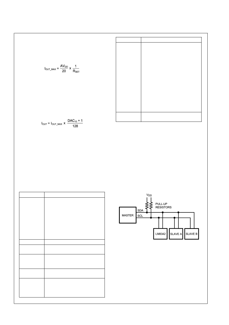
operates as a slave. A typical system using an I
2
C
compatible interface bus is given in
Figure 5
.
The LM8342 can be used in an I
2
C compatible system. All
specifications of the LM8342, dealing with the interface bus,
are guaranteed by design. Except for the bus speed, which
is specified in the Electrical Characteristics table.
KEY ASPECT OF I
2
C COMPATIBLE COMMUNICATION
In this section a brief overview is presented, discussing the
key aspect of I
2
C compatible communication.
Figure 6
shows the timing aspects of the I
2
C compatible serial
interface.
20139231
FIGURE 5. System Using an I
2
C compatible Bus
L
www.national.com
11
相關(guān)PDF資料 |
PDF描述 |
|---|---|
| LM8342SD | Programmable TFT VCOM Calibrator with Non-Volatile |
| LM8342SDX | Programmable TFT VCOM Calibrator with Non-Volatile |
| LM883E | 3-Terminal Adjustable Regulator |
| LM883K | 3-Terminal Adjustable Regulator |
| LM883HVKSTL | 3-Terminal Adjustable Regulator |
相關(guān)代理商/技術(shù)參數(shù) |
參數(shù)描述 |
|---|---|
| LM8342SD | 功能描述:板上安裝溫度傳感器 RoHS:否 制造商:Omron Electronics 輸出類(lèi)型:Digital 配置: 準(zhǔn)確性:+/- 1.5 C, +/- 3 C 溫度閾值: 數(shù)字輸出 - 總線接口:2-Wire, I2C, SMBus 電源電壓-最大:5.5 V 電源電壓-最小:4.5 V 最大工作溫度:+ 50 C 最小工作溫度:0 C 關(guān)閉: 安裝風(fēng)格: 封裝 / 箱體: 設(shè)備功能:Temperature and Humidity Sensor |
| LM8342SD/NOPB | 功能描述:板上安裝溫度傳感器 RoHS:否 制造商:Omron Electronics 輸出類(lèi)型:Digital 配置: 準(zhǔn)確性:+/- 1.5 C, +/- 3 C 溫度閾值: 數(shù)字輸出 - 總線接口:2-Wire, I2C, SMBus 電源電壓-最大:5.5 V 電源電壓-最小:4.5 V 最大工作溫度:+ 50 C 最小工作溫度:0 C 關(guān)閉: 安裝風(fēng)格: 封裝 / 箱體: 設(shè)備功能:Temperature and Humidity Sensor |
| LM8342SDX | 功能描述:板上安裝溫度傳感器 RoHS:否 制造商:Omron Electronics 輸出類(lèi)型:Digital 配置: 準(zhǔn)確性:+/- 1.5 C, +/- 3 C 溫度閾值: 數(shù)字輸出 - 總線接口:2-Wire, I2C, SMBus 電源電壓-最大:5.5 V 電源電壓-最小:4.5 V 最大工作溫度:+ 50 C 最小工作溫度:0 C 關(guān)閉: 安裝風(fēng)格: 封裝 / 箱體: 設(shè)備功能:Temperature and Humidity Sensor |
| LM8342SDX/NOPB | 功能描述:板上安裝溫度傳感器 RoHS:否 制造商:Omron Electronics 輸出類(lèi)型:Digital 配置: 準(zhǔn)確性:+/- 1.5 C, +/- 3 C 溫度閾值: 數(shù)字輸出 - 總線接口:2-Wire, I2C, SMBus 電源電壓-最大:5.5 V 電源電壓-最小:4.5 V 最大工作溫度:+ 50 C 最小工作溫度:0 C 關(guān)閉: 安裝風(fēng)格: 封裝 / 箱體: 設(shè)備功能:Temperature and Humidity Sensor |
| LM8360 | 制造商:未知廠家 制造商全稱(chēng):未知廠家 功能描述: |
發(fā)布緊急采購(gòu),3分鐘左右您將得到回復(fù)。