- 您現(xiàn)在的位置:買賣IC網(wǎng) > PDF目錄385489 > LM8207MTX (NATIONAL SEMICONDUCTOR CORP) TFT 18 Gamma Buffer + VCOM Driver + Voltage Reference PDF資料下載
參數(shù)資料
| 型號: | LM8207MTX |
| 廠商: | NATIONAL SEMICONDUCTOR CORP |
| 元件分類: | 模擬信號調(diào)理 |
| 英文描述: | TFT 18 Gamma Buffer + VCOM Driver + Voltage Reference |
| 中文描述: | SPECIALTY ANALOG CIRCUIT, PDSO48 |
| 封裝: | TSSOP-48 |
| 文件頁數(shù): | 11/22頁 |
| 文件大小: | 1393K |
| 代理商: | LM8207MTX |
Application Section
INTRODUCTION
The performance capabilities of TFT-LCD’s increase rapidly,
with constant improvements such as larger sizes, higher
resolution, and greater brightness. Today’s LCD’s have
screen resolutions of over 1 Mega pixel and higher. The
LM8207 can be used to improve the performance of an LCD.
It is designed for buffering 18 gamma voltage levels and
driving the V
COM
level. These voltage levels can be derived
from a highly stable Voltage Reference, which is included in
the LM8207. The LM8207 meets the design requirements
that combine technical improvement with the demand for
cost effective solutions.
The following sections discuss the principle operation of a
TFT-LCD and the principle operation of the LM8207 which
includes sections on each of the following: the Voltage Ref-
erence, the Gamma Buffers, and the V
Buffer. After this,
the next sections present a typical LM8207 configuration and
consider the maximum power dissipation. The end of this
application section introduces the evaluation board and pre-
sents layout recommendations.
PRINCIPLE OPERATION OF A TFT-LCD
This section offers a brief overview of the principle operating
of TFT-LCD’s. There is a detailed description of how infor-
mation is presented on the display. An explanation of how
data is written to the screen pixels and how the pixels are
selected is also included.
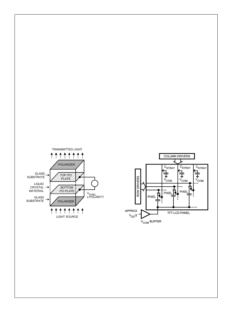
Figure 1
shows a simplified illustration of an individual LCD
pixel. The top and bottom plates of a pixel consist of Indium-
Tin Oxide (ITO), which is a transparent, electrically conduc-
tive material. ITO lies on the inner surfaces of two glass
substrates that are the front and back glass panels of a TFT
display. Sandwiched between two ITO plates is an insulating
material (liquid crystal). This alters the polarization of light,
depending on how much voltage (V
PIXEL
) is applied across
the two plates. Polarizer’s are placed on the outer surfaces
of the two glass substrates. In combination with the liquid
crystal, the polarizer’s create a variable light filter that modu-
lates light transmitted from the back to the front of a display.
A pixel’s bottom plate lies on the backside of a display where
a light source is applied, and the top plate lies on the front,
facing the viewer. For most TFT displays, a pixel transmits
the greatest amount of light when V
≤
±
0.5 V, and it
becomes less transparent as the voltage increases with
either a positive or negative polarity.
For color displays, each pixel is built with three individual sub
pixels. Each sub pixel represents a primary color. These
colors are Red, Green and Blue (RGB). Combining these
three primary colors every user-defined color can be cre-
ated.
Figure 2
shows a simplified diagram of a TFT display, show-
ing how individual pixels are connected to the row, column
and V
driver. Each pixel is represented by a capacitor
with a NMOS transistor connected to its top plate. Pixels in a
TFT panel are arranged in rows and columns. Row lines are
connected to the NMOS gates, and column lines to the
NMOS sources. The back plate of every pixel is connected
to a common voltage called V
. The voltage applied to the
top plates (also called gamma voltage) controls the pixel
brightness. The column drivers supply this gamma voltage
via the column lines, and ‘write’ this voltage to the pixels one
row at a time. This is accomplished by having the row drivers
selecting an individual row of pixels when the column driver
writes the gamma voltage levels. The row drivers sequen-
tially apply a large positive pulse (typically 25V to 35V) to
each row line. This turns on the NMOS transistors connected
to an individual row, allowing voltage from the column lines
to be written to the pixels.
The V
driver (buffer) supplies a common voltage (V
)
to all the pixels in a TFT panel. V
is a constant DC
voltage that is in the middle of the gamma voltage range. As
a result, when a column driver writes to a row of pixels, the
applied voltages are either positive or negative with respect
to V
. In fact, the polarity of a pixel is reversed each time
a row is selected, preventing a pattern from being ‘burned’
into the LCD.
20137930
FIGURE 1. Individual LCD Pixel
20137931
FIGURE 2. TFT Display
L
www.national.com
11
相關(guān)PDF資料 |
PDF描述 |
|---|---|
| LM8261 | RRIO, High Output Current & Unlimited Cap Load Op Amp in SOT23-5 |
| LM8261M5 | RRIO, High Output Current & Unlimited Cap Load Op Amp in SOT23-5 |
| LM8261M5X | RRIO, High Output Current & Unlimited Cap Load Op Amp in SOT23-5 |
| LM8272 | RRIO, High Output Current & Unlimited Cap Load Op Amp in Miniature Package |
| LM8272MM | RRIO, High Output Current & Unlimited Cap Load Op Amp in Miniature Package |
相關(guān)代理商/技術(shù)參數(shù) |
參數(shù)描述 |
|---|---|
| LM8207MTX/NOPB | 功能描述:LCD 驅(qū)動(dòng)器 RoHS:否 制造商:Maxim Integrated 數(shù)位數(shù)量:4.5 片段數(shù)量:30 最大時(shí)鐘頻率:19 KHz 工作電源電壓:3 V to 3.6 V 最大工作溫度:+ 85 C 最小工作溫度:- 20 C 封裝 / 箱體:PDIP-40 封裝:Tube |
| LM825 | 制造商:Pulse Electronics Corporation 功能描述: |
| LM8261 | 制造商:NSC 制造商全稱:National Semiconductor 功能描述:RRIO, High Output Current & Unlimited Cap Load Op Amp in SOT23-5 |
| LM8261M5 | 功能描述:運(yùn)算放大器 - 運(yùn)放 RoHS:否 制造商:STMicroelectronics 通道數(shù)量:4 共模抑制比(最小值):63 dB 輸入補(bǔ)償電壓:1 mV 輸入偏流(最大值):10 pA 工作電源電壓:2.7 V to 5.5 V 安裝風(fēng)格:SMD/SMT 封裝 / 箱體:QFN-16 轉(zhuǎn)換速度:0.89 V/us 關(guān)閉:No 輸出電流:55 mA 最大工作溫度:+ 125 C 封裝:Reel |
| LM8261M5 | 制造商:Texas Instruments 功能描述:OP AMP HIGH O/P RRI/O SMD 8261 |
發(fā)布緊急采購,3分鐘左右您將得到回復(fù)。