- 您現(xiàn)在的位置:買賣IC網(wǎng) > PDF目錄30756 > LM4900M/NOPB (NATIONAL SEMICONDUCTOR CORP) 0.675 W, 1 CHANNEL, AUDIO AMPLIFIER, PDSO8 PDF資料下載
參數(shù)資料
| 型號: | LM4900M/NOPB |
| 廠商: | NATIONAL SEMICONDUCTOR CORP |
| 元件分類: | 音頻/視頻放大 |
| 英文描述: | 0.675 W, 1 CHANNEL, AUDIO AMPLIFIER, PDSO8 |
| 封裝: | SOP-8 |
| 文件頁數(shù): | 11/17頁 |
| 文件大?。?/td> | 843K |
| 代理商: | LM4900M/NOPB |
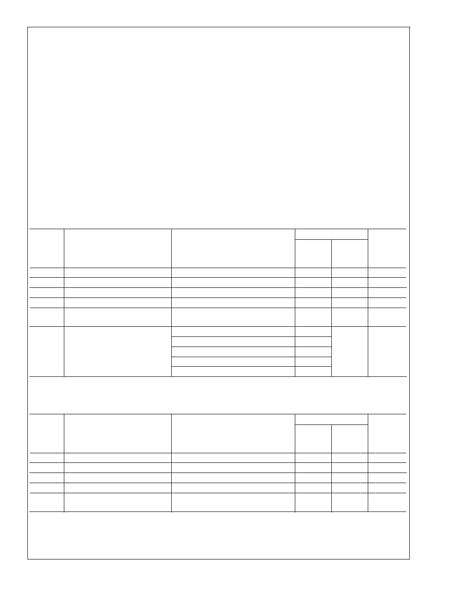
Absolute Maximum Ratings (Note 2)
If Military/Aerospace specified devices are required,
please contact the National Semiconductor Sales Office/
Distributors for availability and specifications.
Supply Voltage
6.0V
Storage Temperature
65C to +150C
Input Voltage
0.3V to V
DD +
0.3V
Power Dissipation (Note 3)
Internally limited
ESD Susceptibility (Note 4)
2000V
ESD Susceptibility (Note 5)
200V
Junction Temperature
150C
Soldering Information
Small Outline Package
Vapor Phase (60 sec.)
215C
Infrared (15 sec.)
220C
See AN-450 “Surface Mounting and their Effects on
Product Reliability” for other methods of soldering surface
mount devices.
Thermal Resistance
θ
JC (M08A)
35C/W
θ
JA (M08A)
170C/W
θ
JC (MUA08A)
56C/W
θ
JA (MUA08A)
190C/W
θ
JA (LDA08B)
67C/W
Operating Ratings
Temperature Range
T
MIN
≤ T
A
≤ T
MAX
40C
≤ T
A
≤
+85C
Supply Voltage
2.0V
≤ V
DD
≤ 5.5V
Electrical Characteristics (Note 1) (Note 2)
The following specifications apply for V
DD = 5V, for all available packages, unless otherwise specified. Limits apply for TA =
25C
Symbol
Parameter
Conditions
LM4900
Units
(Limits)
Typical
Limit
(Notes 7,
I
DD
Quiescent Power Supply Current
V
4
6.0
mA (max)
I
SD
Shutdown Current
V
PIN1 =VDD
0.1
5
A (max)
V
OS
Output Offset Voltage
V
IN = 0V
5
50
mV (max)
P
O
Output Power
THD = 1% (max); f = 1kHz; R
L =8
;
675
300
mW (min)
THD+N
Total Harmonic Distortion+Noise
P
O = 400 mWrms; AVD =2;RL =8
;
20Hz
≤ f ≤ 20kHz, BW < 80kHz
0.4
%
PSRR
Power Supply Rejection Ratio
V
RIPPLE = 200mV sine p-p
dB
f = 217Hz (Note 10)
70
f = 1KHz (Note 10)
67
f = 217Hz (Note 11)
55
f = 1KHz (Note 11)
55
Electrical Characteristics (Note 1) (Note 2)
The following specifications apply for V
DD = 3.3V, for all available packages, unless otherwise specified. Limits apply for TA =
25C
Symbol
Parameter
Conditions
LM4900
Units
(Limits)
Typical
Limit
(Notes 7,
I
DD
Quiescent Power Supply Current
V
3
5
mA (max)
I
SD
Shutdown Current
V
PIN1 =VDD
0.1
3
A (max)
V
OS
Output Offset Voltage
V
IN = 0V
5
50
mV (max)
P
O
Output Power
THD = 1% (max); f = 1kHz; R
L =8
;
265
mW (min)
THD+N
Total Harmonic Distortion+Noise
P
O = 250 mWrms; AVD =2;RL =8
;
20Hz
≤ f ≤ 20kHz, BW < 80kHz
0.4
%
LM4900
www.national.com
3
相關(guān)PDF資料 |
PDF描述 |
|---|---|
| LM4900LD/NOPB | 0.675 W, 1 CHANNEL, AUDIO AMPLIFIER, PDSO8 |
| LM4900MMX/NOPB | 0.675 W, 1 CHANNEL, AUDIO AMPLIFIER, PDSO8 |
| LM4900MX/NOPB | 0.675 W, 1 CHANNEL, AUDIO AMPLIFIER, PDSO8 |
| LM4900LDX/NOPB | 0.675 W, 1 CHANNEL, AUDIO AMPLIFIER, PDSO8 |
| LM4901IBPX | 1.05 W, 1 CHANNEL, AUDIO AMPLIFIER, PBGA9 |
相關(guān)代理商/技術(shù)參數(shù) |
參數(shù)描述 |
|---|---|
| LM4901 | 制造商:未知廠家 制造商全稱:未知廠家 功能描述: |
| LM4901AUL WAF | 制造商:Texas Instruments 功能描述: |
| LM4901IBL | 制造商:未知廠家 制造商全稱:未知廠家 功能描述:AUDIO AMPLIFIER|SINGLE|BGA|9PIN|PLASTIC |
| LM4901IBLX | 制造商:未知廠家 制造商全稱:未知廠家 功能描述:AUDIO AMPLIFIER|SINGLE|BGA|9PIN|PLASTIC |
| LM4901IBP | 制造商:未知廠家 制造商全稱:未知廠家 功能描述:AUDIO AMPLIFIER|SINGLE|BGA|8PIN|PLASTIC |
發(fā)布緊急采購,3分鐘左右您將得到回復(fù)。