- 您現(xiàn)在的位置:買賣IC網(wǎng) > PDF目錄361029 > LM4865M (NATIONAL SEMICONDUCTOR CORP) 750 mW Audio Power Amplifier with DC Volume Control and Headphone Switch PDF資料下載
參數(shù)資料
| 型號: | LM4865M |
| 廠商: | NATIONAL SEMICONDUCTOR CORP |
| 元件分類: | 音頻控制 |
| 英文描述: | 750 mW Audio Power Amplifier with DC Volume Control and Headphone Switch |
| 中文描述: | 1 CHANNEL(S), VOLUME CONTROL CIRCUIT, PDSO8 |
| 封裝: | SOIC-8 |
| 文件頁數(shù): | 7/9頁 |
| 文件大小: | 340K |
| 代理商: | LM4865M |

Application Information
(Continued)
Selection of Input Capacitor Size
Large input capacitors are both expensive and space hungry
for portable designs. Clearly, a certain sized capacitor is
needed to couple in low frequencies without severe attenua-
tion. But in many cases the speakers used in portable sys-
tems, whether internal or external, have little ability to repro-
duce signals below 150 Hz. In this case using a large input
capacitor may not increase system performance.
Besides minimizing the input capacitor size, careful consid-
eration should be paid to the bypass capacitor value. Bypass
capacitor, C
, is the most critical compoment to minimize
turn-on pops since it determines how fast the LM4865 turns
on. The slower the LM4865’s outputs ramp to their quiescent
DC voltage (nominally 1/2 V
), the smaller the turn-on pop.
Choosing C
equal to 1.0 μF along with a small value of C
i
(in the range of 0.1 μF to 0.39 μF), should produce a click-
less and popless shutdown function.Pick C
i
as small as pos-
sible as to minimize clicks and pops.
Click And Pop Circuitry
The LM4865 contains circuitry to minimize turn-on and shut-
down transients or “clicks and pops”. In this case, turn-on re-
fers to either power supply turn-on or the device coming out
of shutdown mode. When the device is turning on, the ampli-
fiers are internally configured as unity gain buffers. An inter-
nal current source ramps up the voltage of the bypass pin.
Both the inputs and outputs ideally track the voltage at the
bypass pin. The device will remain in buffer mode until the
bypass pin has reached its half supply voltage, 1/2 V
. As
soon as the bypass node is stable, the device will become
fully operational, where the gain is set by the external volt-
age on the DC Vol/SD pin.
Although the bypass pin current source cannot be modified,
the size of C
can be changed to alter the device turn-on
time and the amount of “clicks and pops”. By increasing the
value of C
the amount of turn-on pop can be reduced. How-
ever, the tradeoff for using a larger bypass capacitor is an in-
crease in turn-on time for this device. There is a linear rela-
tionship between the size of C
and the turn-on time. Here
are some typical turn-on times for a given C
B
:
C
B
0.01 μF
0.1 μF
0.22 μF
0.47 μF
1.0 μF
T
ON
20 ms
200 ms
420 ms
840 ms
2 Sec
In order eliminate “clicks and pops”, all capacitors must be
discharged before turn-on. Rapid switching of VDD may
cause the
″
clicks and pops
″
to be not easily controlled. In a
single-ended configuration, the output coupling capacitor, C
O
, is of particular concern. This capacitor discharges through
internal 20 k
resistors. Depending on the size of C
, the
time constant can be relatively large. To reduce transients in
single-ended mode, an external 1 k
–5 k
resistor can be
placed in parallel with the internal 20 k
resistor. The
tradeoff for using this resistor is an increase in quiescent cur-
rent.
DS101025-34
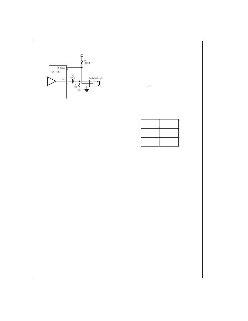
FIGURE 2. Headphone Circuit
L
www.national.com
7
相關(guān)PDF資料 |
PDF描述 |
|---|---|
| LM4865MM | 750 mW Audio Power Amplifier with DC Volume Control and Headphone Switch |
| LM4866 | 2.2W Stereo Audio Amplifier |
| LM4866LQ | 2.2W Stereo Audio Amplifier |
| LM4866MT | 2.2W Stereo Audio Amplifier |
| LM4866MTE | 2.2W Stereo Audio Amplifier |
相關(guān)代理商/技術(shù)參數(shù) |
參數(shù)描述 |
|---|---|
| LM4865M | 制造商:Texas Instruments 功能描述:AMP AUDIO/VOLT CONTROL 0.75W 4865 |
| LM4865M/NOPB | 功能描述:音頻放大器 RoHS:否 制造商:STMicroelectronics 產(chǎn)品:General Purpose Audio Amplifiers 輸出類型:Digital 輸出功率: THD + 噪聲: 工作電源電壓:3.3 V 電源電流: 最大功率耗散: 最大工作溫度: 安裝風(fēng)格:SMD/SMT 封裝 / 箱體:TQFP-64 封裝:Reel |
| LM4865MM | 功能描述:音頻放大器 RoHS:否 制造商:STMicroelectronics 產(chǎn)品:General Purpose Audio Amplifiers 輸出類型:Digital 輸出功率: THD + 噪聲: 工作電源電壓:3.3 V 電源電流: 最大功率耗散: 最大工作溫度: 安裝風(fēng)格:SMD/SMT 封裝 / 箱體:TQFP-64 封裝:Reel |
| LM4865MM/NOPB | 功能描述:音頻放大器 RoHS:否 制造商:STMicroelectronics 產(chǎn)品:General Purpose Audio Amplifiers 輸出類型:Digital 輸出功率: THD + 噪聲: 工作電源電壓:3.3 V 電源電流: 最大功率耗散: 最大工作溫度: 安裝風(fēng)格:SMD/SMT 封裝 / 箱體:TQFP-64 封裝:Reel |
| LM4865MMX | 功能描述:音頻放大器 RoHS:否 制造商:STMicroelectronics 產(chǎn)品:General Purpose Audio Amplifiers 輸出類型:Digital 輸出功率: THD + 噪聲: 工作電源電壓:3.3 V 電源電流: 最大功率耗散: 最大工作溫度: 安裝風(fēng)格:SMD/SMT 封裝 / 箱體:TQFP-64 封裝:Reel |
發(fā)布緊急采購,3分鐘左右您將得到回復(fù)。