- 您現(xiàn)在的位置:買賣IC網(wǎng) > PDF目錄361029 > LM4862N (NATIONAL SEMICONDUCTOR CORP) 675 mW Audio Power Amplifier with Shutdown Mode PDF資料下載
參數(shù)資料
| 型號(hào): | LM4862N |
| 廠商: | NATIONAL SEMICONDUCTOR CORP |
| 元件分類: | 音頻/視頻放大 |
| 英文描述: | 675 mW Audio Power Amplifier with Shutdown Mode |
| 中文描述: | 0.825 W, 1 CHANNEL, AUDIO AMPLIFIER, PDIP8 |
| 封裝: | 0.300 INCH, MDIP-8 |
| 文件頁(yè)數(shù): | 2/10頁(yè) |
| 文件大小: | 262K |
| 代理商: | LM4862N |
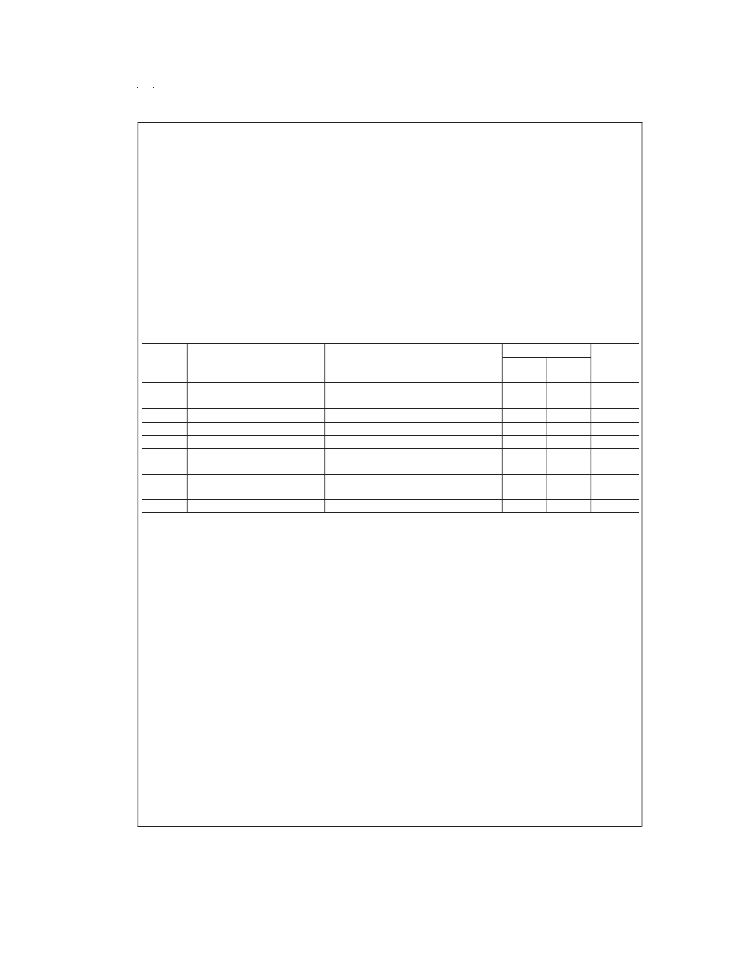
Absolute Maximum Ratings
(Note 2)
If Military/Aerospace specified devices are required,
please contact the National Semiconductor Sales Office/
Distributors for availability and specifications.
Supply Voltage
Storage Temperature
Input Voltage
Power Dissipation (Note 3)
ESD Susceptibility (Note 4)
ESD Susceptibility (Note 5)
Junction Temperature
Soldering Information
Small Outline Package
Vapor Phase (60 sec.)
6.0V
65C to +150C
0.3V to V
DD
+ 0.3V
Internally limited
3500V
250V
150C
215C
Infrared (15 sec.)
See AN-450 “Surface Mounting and their Effects on
Product Reliability” for other methods of soldering surface
mount devices.
Thermal Resistance
θ
JC
(typ)— M08A
θ
JA
(typ)— M08A
θ
JC
(typ)— N08E
θ
JA
(typ)— N08E
220C
35C/W
170C/W
37C/W
107C/W
Operating Ratings
Temperature Range
T
MIN
≤
T
A
≤
T
MAX
Supply Voltage
40C
≤
T
A
≤
85C
2.7V
≤
V
DD
≤
5.5V
Electrical Characteristics
(Note 1) (Note 2)
The following specifications apply for V
DD
= 5V unless otherwise specified. Limits apply for T
A
= 25C.
Symbol
Parameter
Conditions
LM4862
Units
(Limits)
Typical
(Note 6)
Limit
(Note 7)
2.7
5.5
6.0
5
50
500
V
DD
Supply Voltage
V (min)
V (max)
mA (max)
μA (max)
mV (max)
mW (min)
mW
%
I
DD
I
SD
V
OS
P
O
Quiescent Power Supply Current
Shutdown Current
Output Offset Voltage
Output Power
V
IN
= 0V, I
O
= 0A (Note 8)
V
PIN1
= V
DD
V
IN
= 0V
THD = 1% (max); f = 1 kHz; R
L
= 8
THD + N = 10%; f = 1 kHz; R
L
= 8
P
O
= 500 mWrms; R
L
= 8
A
VD
= 2; 20 Hz
≤
f
≤
20 kHz
V
DD
= 4.9V to 5.1V
3.6
0.7
5
675
825
0.55
THD + N
Total Harmonic Distortion +
Noise
Power Supply Rejection Ratio
PSRR
50
dB
Note 1:
All voltages are measured with respect to the ground pin, unless otherwise specified.
Note 2:
Absolute Maximum Ratings indicate limits beyond which damage to the device may occur. Operating Ratings indicate conditions for which the device is func-
tional, but do not guarantee specific performance limits. Electrical Characteristics state DC andAC electrical specifications under particular test conditions which guar-
antee specific performance limits. This assumes that the device is within the Operating Ratings. Specifications are not guaranteed for parameters where no limit is
given, however, the typical value is a good indication of device performance.
Note 3:
The maximum power dissipation must be derated at elevated temperatures and is dictated by T
,
θ
, and the ambient temperature T
. The maximum
allowable power dissipation is P
= (T
T
)/
θ
. For the LM4862, T
= 150C. The typical junction-to-ambient thermal resistance, when board mounted,
is 170C/W for package number M08A and is 107C/W for package number N08E.
Note 4:
Human body model, 100 pF discharged through a 1.5 k
resistor.
Note 5:
Machine Model, 200 pF–240 pF discharged through all pins.
Note 6:
Typicals are measured at 25C and represent the parametric norm.
Note 7:
Limits are guaranteed to National’s AOQL (Average Outgoing Quality Level).
Note 8:
The quiescent power supply current depends on the offset voltage when a practical load is connected to the amplifier.
www.national.com
2
相關(guān)PDF資料 |
PDF描述 |
|---|---|
| LM4862 | 675 mW Audio Power Amplifier with Shutdown Mode |
| LM4862M | 675 mW Audio Power Amplifier with Shutdown Mode |
| LM4863 | Dual 2.2W Audio Amplifier Plus Stereo Headphone Function |
| LM4863M | Dual 2.2W Audio Amplifier Plus Stereo Headphone Function |
| LM4863MT | Dual 2.2W Audio Amplifier Plus Stereo Headphone Function |
相關(guān)代理商/技術(shù)參數(shù) |
參數(shù)描述 |
|---|---|
| LM4863 | 制造商:未知廠家 制造商全稱:未知廠家 功能描述:Dual 2.2W Audio Amplifier Plus Stereo Headphone Function |
| LM4863_06 | 制造商:NSC 制造商全稱:National Semiconductor 功能描述:Dual 2.2W Audio Amplifier Plus Stereo Headphone Function |
| LM4863A EA WAF | 制造商:Texas Instruments 功能描述: |
| LM4863-D16-T | 制造商:UTC-IC 制造商全稱:UTC-IC 功能描述:DUAL 2.2W AUDIO AMPLIFIER PLUS STEREO HEADPHONE FUNCTION |
| LM4863LQ | 功能描述:音頻放大器 RoHS:否 制造商:STMicroelectronics 產(chǎn)品:General Purpose Audio Amplifiers 輸出類型:Digital 輸出功率: THD + 噪聲: 工作電源電壓:3.3 V 電源電流: 最大功率耗散: 最大工作溫度: 安裝風(fēng)格:SMD/SMT 封裝 / 箱體:TQFP-64 封裝:Reel |
發(fā)布緊急采購(gòu),3分鐘左右您將得到回復(fù)。