- 您現(xiàn)在的位置:買賣IC網(wǎng) > PDF目錄358865 > LM4666SDA (National Semiconductor Corporation) Filterless High Efficiency Stereo 1.2W Switching Audio Amplifier PDF資料下載
參數(shù)資料
| 型號(hào): | LM4666SDA |
| 廠商: | National Semiconductor Corporation |
| 元件分類: | 音頻放大器 |
| 英文描述: | Filterless High Efficiency Stereo 1.2W Switching Audio Amplifier |
| 中文描述: | 濾波1.2W的立體聲高效率開關(guān)音頻放大器 |
| 文件頁(yè)數(shù): | 4/15頁(yè) |
| 文件大?。?/td> | 642K |
| 代理商: | LM4666SDA |
第1頁(yè)第2頁(yè)第3頁(yè)當(dāng)前第4頁(yè)第5頁(yè)第6頁(yè)第7頁(yè)第8頁(yè)第9頁(yè)第10頁(yè)第11頁(yè)第12頁(yè)第13頁(yè)第14頁(yè)第15頁(yè)
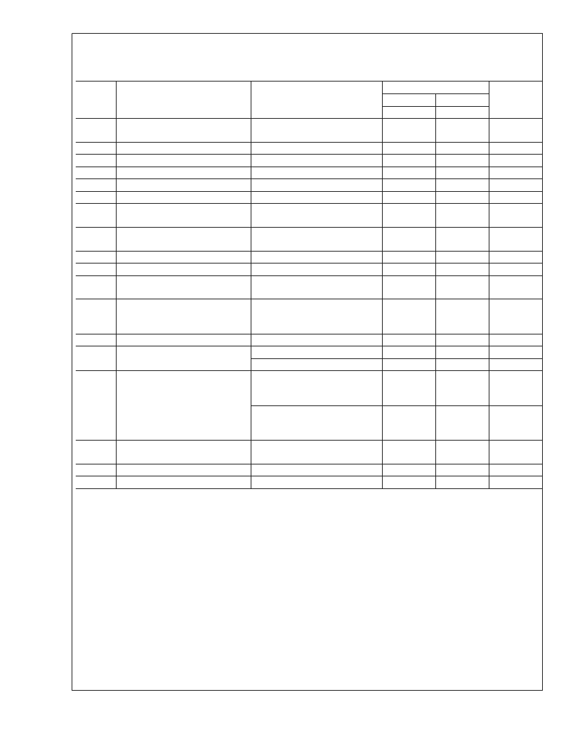
Electrical Characteristics V
DD
= 3V
The following specifications apply for V
DD
= 3V and R
L
= 15μH + 8
+ 15μH unless otherwise specified. Limits apply for T
A
=
25C.
(Notes 1, 2)
Symbol
Parameter
Conditions
LM4666
Units
(Limits)
Typical
(Note 6)
6.5
7.0
0.02
1.0
0.8
1.0
0.8
Limit
(Notes 7, 8)
I
DD
Quiescent Power Supply Current
V
IN
= 0V, No Load
V
IN
= 0V, R
L
= 15μH + 8
+ 15μH
V
SD
= GND (Note 9)
10
mA (max)
I
SD
V
SDIH
V
SDIL
V
GSIH
V
GSIL
Shutdown Current
Shutdown Voltage Input High
Shutdown Voltage Input Low
Gain Select Input High
Gain Select Input Low
2.0
1.4
0.4
1.4
0.4
5.25
6.75
11.25
12.75
35
μA (max)
V (min)
V (max)
V (min)
V (max)
dB (min)
dB (max)
dB (min)
dB (max)
mV (max)
ms
A
V
Closed Loop Gain
V
Gain Select
= V
DD
6
A
V
Closed Loop Gain
V
Gain Select
= GND
12
V
OS
T
WU
Output Offset Voltage
Wake-up Time
10
6
P
o
Output Power
THD = 1% (max); f = 1kHz,
22kHz BW
P
O
= 100mW
RMS
/Channel,
f
IN
= 1kHz, 22kHz BW,
Both channels in phase
P
O
= 100mW
RMS
, f = 1kHz
V
Gain Select
= V
DD
V
Gain Select
= GND
V
ripple
= 100mV
RMS
sine wave,
f
RIPPLE
= 217Hz,
Inputs terminated to AC GND
V
Ripple
= 100mV
RMS
sine wave,
f
RIPPLE
= 217Hz,
P
OUT
= 10mW,1kHz
V
Ripple
= 100mV
RMS
,
f
Ripple
= 217Hz, Input referred
P
O
= 400mW
RMS
, A-Weighted Filter
A-Weighted filter, V
in
= 0V
450
400
mW (min)
THD+N
Total Harmonic Distortion+Noise
0.65
%
X
TALK
Channel Separation
57
90
60
dB
k
k
R
IN
Differential Input Resistance
PSRR
Power Supply Rejection Ratio
60
dB
65
dB
CMRR
Common Mode Rejection Ratio
48
dB
SNR
Signal to Noise Ratio
Output Noise
83
125
dB
μV
e
OUT
Note 1:
All voltages are measured with respect to the ground pin, unless otherwise specified.
Note 2:
Absolute Maximum Ratings
indicate limits beyond which damage to the device may occur.
Operating Ratings
indicate conditions for which the device is
functional, but do not guarantee specific performance limits.
Electrical Characteristics
state DC andAC electrical specifications under particular test conditions which
guarantee specific performance limits. This assumes that the device is within the Operating Ratings. Specifications are not guaranteed for parameters where no limit
is given, however, the typical value is a good indication of device performance.
Note 3:
The maximum power dissipation must be derated at elevated temperatures and is dictated by T
JMAX
,
θ
JA
, and the ambient temperature T
A
. The maximum
allowable power dissipation is P
DMAX
= (T
JMAX
–T
A
)/
θ
JA
or the number given in Absolute Maximum Ratings, whichever is lower. For the LM4666, T
JMAX
= 150C.
The typical
θ
JA
is 63C/W and the typical
θ
JC
is 12C/W for the SDA package.
Note 4:
Human body model, 100pF discharged through a 1.5k
resistor.
Note 5:
Machine Model, 220pF – 240pF discharged through all pins.
Note 6:
Typical specifications are specified at 25C and represent the parametric norm.
Note 7:
Tested limits are guaranteed to National’s AOQL (Average Outgoing Quality Level).
Note 8:
Datasheet min/max specification limits are guaranteed by design, test, or statistical analysis.
Note 9:
Shutdown current is measured in a normal room environment. Exposure to direct sunlight will increase I
by a maximum of 2μA. The Shutdown pin should
be driven as close as possible to GND for minimal shutdown current and to V
DD
for the best THD performance in PLAY mode. See the
Application Information
section under SHUTDOWN FUNCTION for more information.
Note 10:
The performance graphs were taken using the Audio Precision AUX–0025 Switching Amplifier Measurement Filter in series with the LC filter on the demo
board.
L
www.national.com
4
相關(guān)PDF資料 |
PDF描述 |
|---|---|
| LM4668 | 10W High-Efficiency Mono BTL Audio Power Amplifier |
| LM4668LD | 10W High-Efficiency Mono BTL Audio Power Amplifier |
| LM4668MH | 10W High-Efficiency Mono BTL Audio Power Amplifier |
| LM4670 | Filterless High Efficiency 3W Switching Audio Amplifier |
| LM4670ITL | Filterless High Efficiency 3W Switching Audio Amplifier |
相關(guān)代理商/技術(shù)參數(shù) |
參數(shù)描述 |
|---|---|
| LM4666SDBD | 功能描述:音頻 IC 開發(fā)工具 LM4666SD EVAL BOARD RoHS:否 制造商:Texas Instruments 產(chǎn)品:Evaluation Kits 類型:Audio Amplifiers 工具用于評(píng)估:TAS5614L 工作電源電壓:12 V to 38 V |
| LM4666SDBD/NOPB | 功能描述:音頻 IC 開發(fā)工具 LM4666 Eval Brd RoHS:否 制造商:Texas Instruments 產(chǎn)品:Evaluation Kits 類型:Audio Amplifiers 工具用于評(píng)估:TAS5614L 工作電源電壓:12 V to 38 V |
| LM4666SDX | 功能描述:音頻放大器 RoHS:否 制造商:STMicroelectronics 產(chǎn)品:General Purpose Audio Amplifiers 輸出類型:Digital 輸出功率: THD + 噪聲: 工作電源電壓:3.3 V 電源電流: 最大功率耗散: 最大工作溫度: 安裝風(fēng)格:SMD/SMT 封裝 / 箱體:TQFP-64 封裝:Reel |
| LM4666SDX/NOPB | 功能描述:音頻放大器 RoHS:否 制造商:STMicroelectronics 產(chǎn)品:General Purpose Audio Amplifiers 輸出類型:Digital 輸出功率: THD + 噪聲: 工作電源電壓:3.3 V 電源電流: 最大功率耗散: 最大工作溫度: 安裝風(fēng)格:SMD/SMT 封裝 / 箱體:TQFP-64 封裝:Reel |
| LM4667 | 制造商:NSC 制造商全稱:National Semiconductor 功能描述:Filterless High Efficiency 1.3W Switching Audio Amplifier |
發(fā)布緊急采購(gòu),3分鐘左右您將得到回復(fù)。