- 您現(xiàn)在的位置:買賣IC網(wǎng) > PDF目錄358865 > LM4664 (National Semiconductor Corporation) Filterless High Efficiency 1.1W Switching Audio Amplifier PDF資料下載
參數(shù)資料
| 型號(hào): | LM4664 |
| 廠商: | National Semiconductor Corporation |
| 元件分類: | 音頻放大器 |
| 英文描述: | Filterless High Efficiency 1.1W Switching Audio Amplifier |
| 中文描述: | 濾波高效率開關(guān)音頻放大器1.1W |
| 文件頁數(shù): | 4/14頁 |
| 文件大小: | 550K |
| 代理商: | LM4664 |
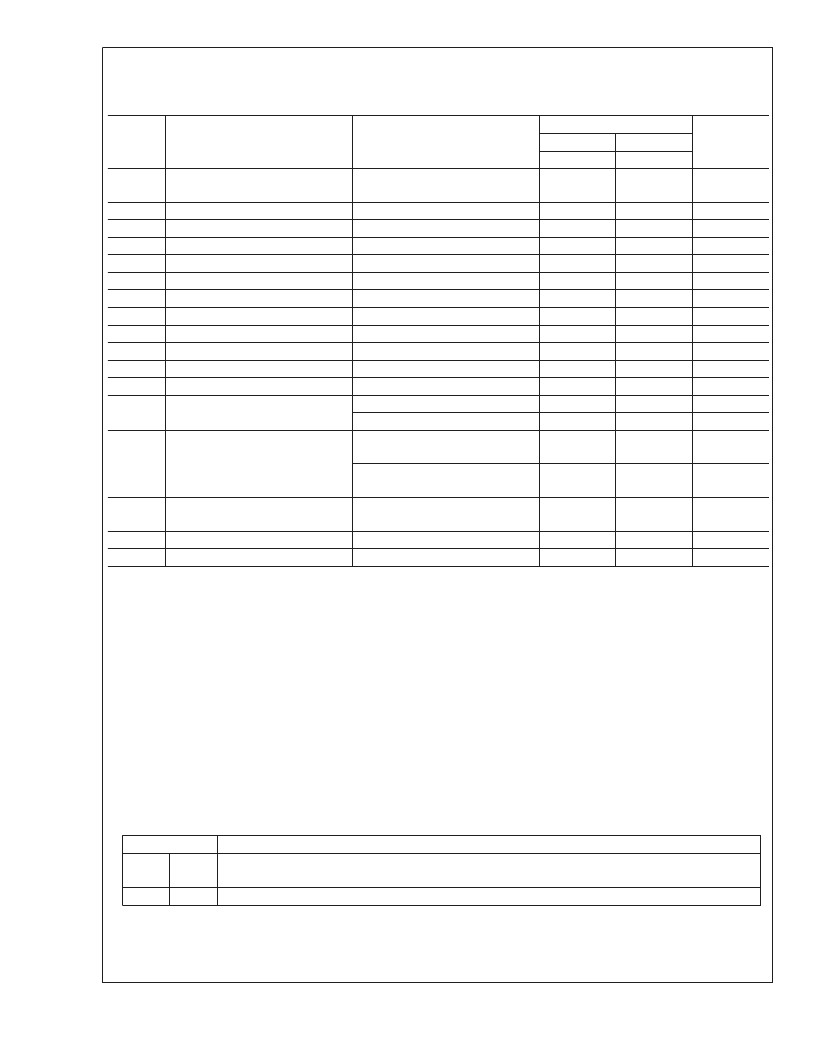
Electrical Characteristics V
DD
= 5V
The following specifications apply for V
DD
= 5V and R
L
= 15μH + 8
+ 15μH unless otherwise specified. Limits apply for T
A
=
25C.
(Notes 1, 2)
Symbol
Parameter
Conditions
LM4664
Units
(Limits)
Typical
(Note 6)
8
9
0.4
1.2
1.1
1.2
1.1
6
12
10
7
1.1
0.8
90
60
55
(f = 217Hz)
65
(f = 217Hz)
41
Limit
(Notes 7, 8)
I
DD
Quiescent Power Supply Current
V
IN
= 0V, No Load
V
IN
= 0V, R
L
= 15μH + 8
+ 15μH
V
SD
= GND (Note 9)
mA
mA
μA
V
V
V
V
dB
dB
mV
ms
W
%
k
k
dB
I
SD
V
SDIH
V
SDIL
V
GSIH
V
GSIL
A
V
A
V
V
OS
T
WU
P
o
THD+N
Shutdown Current
Shutdown Voltage Input High
Shutdown Voltage Input Low
Gain Select Input High
Gain Select Input Low
Closed Loop Gain
Closed Loop Gain
Output Offset Voltage
Wake-up Time
Output Power
Total Harmonic Distortion+Noise
V
Gain Select
= V
DD
V
Gain Select
= GND
THD = 2% (max); f = 1kHz
P
O
= 100mW
RMS
; f
IN
= 1kHz
V
Gain Select
= V
DD
V
Gain Select
= GND
V
ripple
= 100mV
RMS
sine wave
Inputs terminated to GND
V
Ripple
= 100mV
RMS
sine wave
P
OUT
= 10mW,1kHz
V
Ripple
= 100mV
RMS
,
f
Ripple
= 217Hz
P
O
= 1W
RMS
, A-Weighted Filter
A-Weighted filter, V
in
= 0V
R
IN
Differential Input Resistance
PSRR
Power Supply Rejection Ratio
dB
CMRR
Common Mode Rejection Ratio
dB
SNR
Signal to Noise Ratio
Output Noise
83
200
dB
μV
e
OUT
Note 1:
All voltages are measured with respect to the ground pin, unless otherwise specified.
Note 2:
Absolute Maximum Ratings
indicate limits beyond which damage to the device may occur.
Operating Ratings
indicate conditions for which the device is
functional, but do not guarantee specific performance limits.
Electrical Characteristics
state DC andAC electrical specifications under particular test conditions which
guarantee specific performance limits. This assumes that the device is within the Operating Ratings. Specifications are not guaranteed for parameters where no limit
is given, however, the typical value is a good indication of device performance.
Note 3:
The maximum power dissipation must be derated at elevated temperatures and is dictated by T
JMAX
,
θ
JA
, and the ambient temperature T
A
. The maximum
allowable power dissipation is P
DMAX
= (T
JMAX
–T
A
)/
θ
JA
or the number given in Absolute Maximum Ratings, whichever is lower. For the LM4664, T
JMAX
= 150C.
The typical
θ
JA
is 220C/W for the microSMD package.
Note 4:
Human body model, 100pF discharged through a 1.5k
resistor.
Note 5:
Machine Model, 220pF–240pF discharged through all pins.
Note 6:
Typical specifications are specified at 25C and represent the parametric norm.
Note 7:
Tested limits are guaranteed to National’s AOQL (Average Outgoing Quality Level).
Note 8:
Datasheet min/max specification limits are guaranteed by design, test, or statistical analysis.
Note 9:
Shutdown current is measured in a normal room environment. Exposure to direct sunlight will increase I
SD
by a maximum of 2μA. The Shutdown pin should
be driven as close as possible to GND for minimal shutdown current and to V
DD
for the best THD performance in PLAY mode. See the
Application Information
section under SHUTDOWN FUNCTION for more information.
External Components Description
(
Figure 1
)
Components
1.
Functional Description
C
S
Supply bypass capacitor which provides power supply filtering. Refer to the
Power Supply Bypassing
section for information concerning proper placement and selection of the supply bypass capacitor.
Input AC coupling capacitor which blocks the DC voltage at the amplifier’s input terminals.
2.
C
I
L
www.national.com
4
相關(guān)PDF資料 |
PDF描述 |
|---|---|
| LM4665 | Filterless High Efficiency 1W Switching Audio Amplifier |
| LM4665ITLX | Filterless High Efficiency 1W Switching Audio Amplifier |
| LM4665LD | Filterless High Efficiency 1W Switching Audio Amplifier |
| LM4665MM | Filterless High Efficiency 1W Switching Audio Amplifier |
| LM4665ITL | Filterless High Efficiency 1W Switching Audio Amplifier |
相關(guān)代理商/技術(shù)參數(shù) |
參數(shù)描述 |
|---|---|
| LM4664ITL | 制造商:Texas Instruments 功能描述:AMP FILTERLESS CLASS-A 1.1W 4664 |
| LM4665 | 制造商:NSC 制造商全稱:National Semiconductor 功能描述:Filterless High Efficiency 1W Switching Audio Amplifier |
| LM4665 WAF | 制造商:Texas Instruments 功能描述: |
| LM4665B WAF | 制造商:Texas Instruments 功能描述: |
| LM4665ITL | 制造商:Texas Instruments 功能描述:Audio Amp Speaker 1-CH Mono 1.4W Class-AB 9-Pin uSMD T/R 制造商:Texas Instruments 功能描述:1W Class D Switching Amplifier,LM4665ITL |
發(fā)布緊急采購,3分鐘左右您將得到回復(fù)。