- 您現(xiàn)在的位置:買賣IC網(wǎng) > PDF目錄384598 > LM3405AXMKX (NATIONAL SEMICONDUCTOR CORP) 1.6MHz, 1A Constant Current Buck LED Driver with Internal Compensation in Tiny SOT23 Package PDF資料下載
參數(shù)資料
| 型號: | LM3405AXMKX |
| 廠商: | NATIONAL SEMICONDUCTOR CORP |
| 元件分類: | 穩(wěn)壓器 |
| 英文描述: | 1.6MHz, 1A Constant Current Buck LED Driver with Internal Compensation in Tiny SOT23 Package |
| 中文描述: | 2.8 A SWITCHING REGULATOR, 1900 kHz SWITCHING FREQ-MAX, PDSO6 |
| 封裝: | TSOT-23, 6 PIN |
| 文件頁數(shù): | 7/20頁 |
| 文件大小: | 396K |
| 代理商: | LM3405AXMKX |
When the LM3405A starts up, internal circuitry from V
sup-
plies a 20mA current to the BOOST pin, flowing out of the
BOOST pin into C3. This current charges C3 to a voltage suf-
ficient to turn the switch on. The BOOST pin will continue to
source current to C3 until the voltage at the feedback pin is
greater than 123mV.
There are various methods to derive V
BOOST
:
1.
From the input voltage (V
IN
)
2.
From the output voltage (V
OUT
)
3.
From a shunt or series zener diode
4.
From an external distributed voltage rail (V
EXT
)
The first method is shown in the Simplified Block Diagram of
Figure 1
. Capacitor C3 is charged via diode D2 by V
. During
a normal switching cycle, when the internal NMOS power
switch is off (T
) (refer to
Figure 2
), V
equals V
mi-
nus the forward voltage of D2 (V
), during which the current
in the inductor (L1) forward biases the catch diode D1 (V
D1
).
Therefore the gate drive voltage stored across C3 is:
V
BOOST
- V
SW
= V
IN
- V
D2
+ V
D1
When the NMOS switch turns on (T
ON
), the switch pin rises
to:
V
SW
= V
IN
– (R
DS(ON)
x I
L
)
Since the voltage across C3 remains unchanged, V
BOOST
is
forced to rise thus reverse biasing D2. The voltage at
V
BOOST
is then:
V
BOOST
= 2V
IN
– (R
DS(ON)
x I
L
) – V
D2
+ V
D1
Depending on the quality of the diodes D1 and D2, the gate
drive voltage in this method can be slightly less or larger than
the input voltage V
. For best performance, ensure that the
variation of the input supply does not cause the gate drive
voltage to fall outside the recommended range:
2.5V < V
IN
- V
D2
+ V
D1
< 5.5V
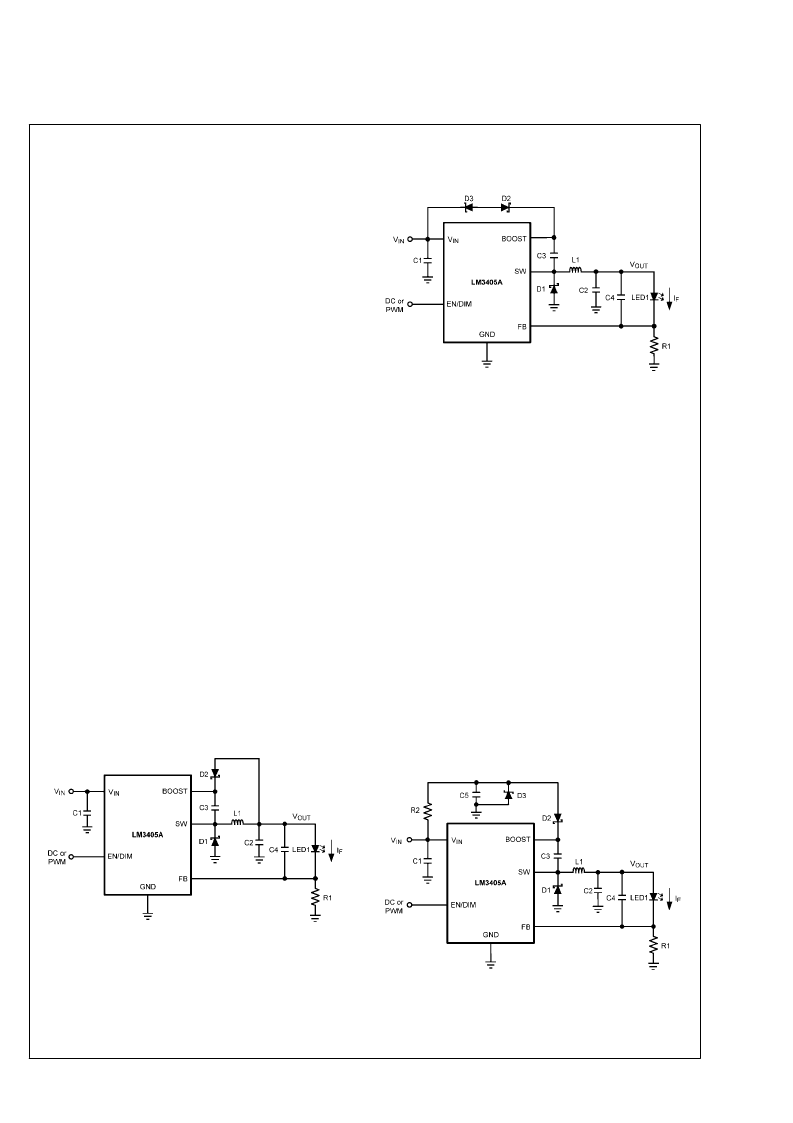
The second method for deriving the boost voltage is to con-
nect D2 to the output as shown in
Figure 3
. The gate drive
voltage in this configuration is:
V
BOOST
- V
SW
= V
OUT
– V
D2
+ V
D1
Since the gate drive voltage needs to be in the range of 2.5V
to 5.5V, the output voltage V
should be limited to a certain
range. For the calculation of V
OUT
, see OUTPUT VOLTAGE
section.
30015293
FIGURE 3. V
BOOST
derived from V
OUT
The third method can be used in the applications where both
V
and V
are greater than 5.5V. In these cases, C3 cannot
be charged directly from these voltages; instead C3 can be
charged from V
IN
or V
OUT
minus a zener voltage (V
D3
) by
placing a zener diode D3 in series with D2 as shown in
Figure
4
. When using a series zener diode from the input, the gate
drive voltage is V
IN
- V
D3
- V
D2
+ V
D1
.
30015299
FIGURE 4. V
BOOST
derived from V
IN
through a Series
Zener
An alternate method is to place the zener diode D3 in a shunt
configuration as shown in
Figure 5
. A small 350mW to
500mW, 5.1V zener in a SOT-23 or SOD package can be
used for this purpose. A small ceramic capacitor such as a
6.3V, 0.1μF capacitor (C5) should be placed in parallel with
the zener diode. When the internal NMOS switch turns on, a
pulse of current is drawn to charge the internal NMOS gate
capacitance. The 0.1μF parallel shunt capacitor ensures that
the V
voltage is maintained during this time. Resistor R2
should be chosen to provide enough RMS current to the zener
diode and to the BOOST pin. A recommended choice for the
zener current (I
) is 1mA. The current I
into the
BOOST pin supplies the gate current of the NMOS power
switch. It reaches a maximum of around 3.6mA at the highest
gate drive voltage of 5.5V over the LM3405A operating range.
For the worst case I
, increase the current by 50%. In
that case, the maximum boost current will be:
I
BOOST-MAX
= 1.5 x 3.6mA = 5.4mA
R2 will then be given by:
R2 = (V
IN
- V
ZENER
) / (I
BOOST_MAX
+ I
ZENER
)
For example, let V
IN
= 12V, V
ZENER
= 5V, I
ZENER
= 1mA, then:
R2 = (12V - 5V) / (5.4mA + 1mA) = 1.09k
30015294
FIGURE 5. V
BOOST
derived from V
IN
through a Shunt Zener
7
www.national.com
L
相關(guān)PDF資料 |
PDF描述 |
|---|---|
| LM3407 | 350 mA, Constant Current Output Floating Buck Switching Converter for High Power LEDs |
| LM3407MY | 350 mA, Constant Current Output Floating Buck Switching Converter for High Power LEDs |
| LM3407MYX | 350 mA, Constant Current Output Floating Buck Switching Converter for High Power LEDs |
| LM3410YSDX | 525kHz/1.6MHz, Constant Current Boost and SEPIC LED Driver with Internal Compensation |
| LM3410 | 525kHz/1.6MHz, Constant Current Boost and SEPIC LED Driver with Internal Compensation |
相關(guān)代理商/技術(shù)參數(shù) |
參數(shù)描述 |
|---|---|
| LM3405AXMKX/NOPB | 功能描述:LED照明驅(qū)動器 RoHS:否 制造商:STMicroelectronics 輸入電壓:11.5 V to 23 V 工作頻率: 最大電源電流:1.7 mA 輸出電流: 最大工作溫度: 安裝風(fēng)格:SMD/SMT 封裝 / 箱體:SO-16N |
| LM3405AXMY | 制造商:Texas Instruments 功能描述:LED DRVR 3.3V/5V/9V/12V/15V/18V 8-Pin MSOP T/R 制造商:Texas Instruments 功能描述:LED DRIVER, 1A, BUCK, 1.6MHZ, 8MSOP 制造商:Texas Instruments 功能描述:LED DRIVER, 1A, BUCK, 1.6MHZ, 8MSOP; Topology:Buck; No. of Outputs:1; Output Current:1A; Output Voltage:20V; Driver Case Style:MSOP; Input Voltage Min:3V; Input Voltage Max:22V; Dimming Control Type:PWM; Switching Frequency:1.6MHz; ;RoHS Compliant: Yes |
| LM3405AXMY/NOPB | 功能描述:LED照明驅(qū)動器 RoHS:否 制造商:STMicroelectronics 輸入電壓:11.5 V to 23 V 工作頻率: 最大電源電流:1.7 mA 輸出電流: 最大工作溫度: 安裝風(fēng)格:SMD/SMT 封裝 / 箱體:SO-16N |
| LM3405AXMYEVAL | 功能描述:電源管理IC開發(fā)工具 LM3405AXMY EVAL BOARD RoHS:否 制造商:Maxim Integrated 產(chǎn)品:Evaluation Kits 類型:Battery Management 工具用于評估:MAX17710GB 輸入電壓: 輸出電壓:1.8 V |
| LM3405AXMYEVAL | 制造商:Texas Instruments 功能描述:LM3405AXMY EVAL BOARD |
發(fā)布緊急采購,3分鐘左右您將得到回復(fù)。