- 您現(xiàn)在的位置:買賣IC網(wǎng) > PDF目錄358840 > LM323 (ON SEMICONDUCTOR) 5.0 AMP POSITIVE VOLTAGE REGULATOR PDF資料下載
參數(shù)資料
| 型號: | LM323 |
| 廠商: | ON SEMICONDUCTOR |
| 元件分類: | 基準電壓源/電流源 |
| 英文描述: | 5.0 AMP POSITIVE VOLTAGE REGULATOR |
| 中文描述: | 5.0放大器正電壓穩(wěn)壓器 |
| 文件頁數(shù): | 2/8頁 |
| 文件大小: | 126K |
| 代理商: | LM323 |
LM323, A
2
MOTOROLA ANALOG IC DEVICE DATA
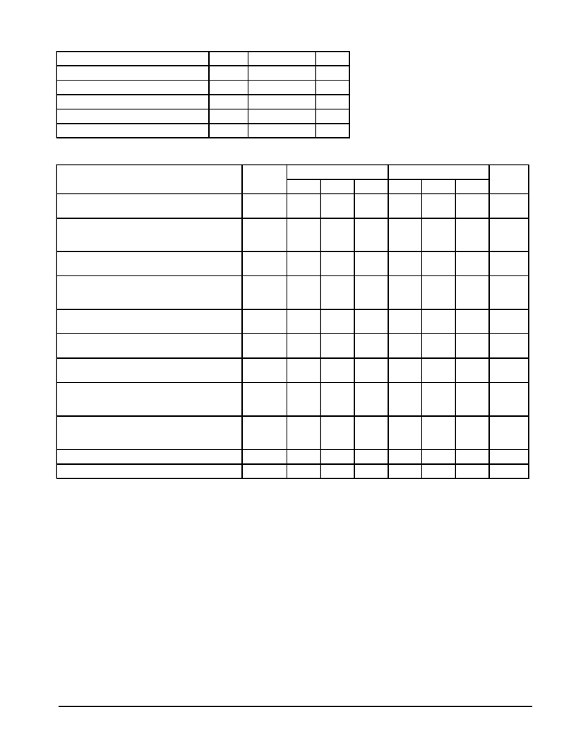
MAXIMUM RATINGS
Rating
Symbol
Value
Unit
Input Voltage
Vin
PD
TJ
Tstg
Tsolder
20
Vdc
Power Dissipation
Internally Limited
W
Operating Junction Temperature Range
0 to +125
°
C
Storage Temperature Range
–65 to +150
°
C
Lead Temperature (Soldering, 10 s)
300
°
C
ELECTRICAL CHARACTERISTICS
(TJ = Tlow to Thigh [Note 1], unless otherwise noted.)
LM323A
LM323
Characteristics
Symbol
Min
Typ
Max
Min
Typ
Max
Unit
Output Voltage
(Vin = 7.5 V, 0
≤
Iout
≤
3.0 A, TJ = 25
°
C)
VO
4.9
5.0
5.1
4.8
5.0
5.2
V
Output Voltage
(7.5 V
≤
Vin
≤
15 V, 0
≤
Iout
≤
3.0 A,
P
≤
Pmax) (Note 2)
VO
4.8
5.0
5.2
4.75
5.0
5.25
V
Line Regulation
(7.5 V
≤
Vin
≤
15 V, TJ = 25
°
C) (Note 3)
Regline
–
1.0
15
–
1.0
25
mV
Load Regulation
(Vin = 7.5 V, 0
≤
Iout
≤
3.0 A, TJ = 25
°
C)
(Note 3)
Regload
–
10
50
–
10
100
mV
Thermal Regulation
(Pulse = 10 ms, P = 20 W, TA = 25
°
C)
Regtherm
–
0.001
0.01
–
0.002
0.03
%VO/W
Quiescent Current
(7.5 V
≤
Vin
≤
15 V, 0
≤
Iout
≤
3.0 A)
IB
–
3.5
10
–
3.5
20
mA
Output Noise Voltage
(10 Hz
≤
f
≤
100 kHz, TJ = 25
°
C)
VN
–
40
–
–
40
–
μ
Vrms
Ripple Rejection
(8.0 V
≤
Vin
≤
18 V, Iout = 2.0A,
f = 120 Hz, TJ = 25
°
C)
RR
66
75
–
62
75
–
dB
Short Circuit Current Limit
(Vin = 15 V, TJ = 25
°
C)
(Vin = 7.5 V, TJ = 25
°
C)
ISC
–
–
4.5
5.5
–
–
–
–
4.5
5.5
–
–
A
Long Term Stability
S
–
–
35
–
–
35
mV
Thermal Resistance, Junction–to–Case (Note 4)
R
Θ
JC
–
2.0
–
–
2.0
–
°
C/W
NOTES:
1.Tlow to Thigh = 0
°
to +125
°
C
2.Although power dissipation is internally limited, specifications apply only for P
≤
Pmax = 25 W.
3.Load and line regulation are specified at constant junction temperature. Pulse testing is required with a pulse width
≤
1.0 ms and a duty cycle
≤
5%.
4.Without a heatsink, the thermal resistance (R
JA is 65
°
C/W). With a heatsink, the effective thermal resistance can approach the specified values of
2.0
°
C/W, depending on the efficiency of the heatsink.
相關PDF資料 |
PDF描述 |
|---|---|
| LM324KANS | QUADRUPLE OPERATIONAL AMPLIFIERS |
| LM2902MX | Voltage-Feedback Operational Amplifier |
| LM324DH | Low power quad op amps |
| LM2902DBR | OP-AMP|QUAD|BIPOLAR|SSOP|14PIN|PLASTIC |
| LM324A | Low power quad op amps |
相關代理商/技術參數(shù) |
參數(shù)描述 |
|---|---|
| LM323/D | 制造商:未知廠家 制造商全稱:未知廠家 功能描述:Positive Voltage Regulators |
| LM323_02 | 制造商:ONSEMI 制造商全稱:ON Semiconductor 功能描述:3.0 A Positive Voltage Regulators |
| LM323_08 | 制造商:STMICROELECTRONICS 制造商全稱:STMicroelectronics 功能描述:Three-terminal 3 A adjustable voltage regulators |
| LM323-155.52M | 制造商:CONNOR-WINFIELD 制造商全稱:Connor-Winfield Corporation 功能描述:5.0x7.0mm Surface Mount LVDS Clock Oscillator Series |
| LM323A | 制造商:NSC 制造商全稱:National Semiconductor 功能描述:3-Amp, 5-Volt Positive Regulator |
發(fā)布緊急采購,3分鐘左右您將得到回復。