- 您現(xiàn)在的位置:買賣IC網(wǎng) > PDF目錄44551 > LM2788MM-2.0/NOPB (NATIONAL SEMICONDUCTOR CORP) SWITCHED CAPACITOR REGULATOR, 500 kHz SWITCHING FREQ-MAX, PDSO8 PDF資料下載
參數(shù)資料
| 型號(hào): | LM2788MM-2.0/NOPB |
| 廠商: | NATIONAL SEMICONDUCTOR CORP |
| 元件分類: | 穩(wěn)壓器 |
| 英文描述: | SWITCHED CAPACITOR REGULATOR, 500 kHz SWITCHING FREQ-MAX, PDSO8 |
| 封裝: | MSOP-8 |
| 文件頁(yè)數(shù): | 7/12頁(yè) |
| 文件大小: | 372K |
| 代理商: | LM2788MM-2.0/NOPB |
Electrical Characteristics
J =25
oC.
Limits in boldface type apply over the operating junction temperature range. Unless otherwise specified: 2.6
≤ V
IN
≤ 5.5V,
V(EN) = V
(Continued)
Note 4: Thermal shutdown circuitry protects the device from permanent damage.
Note 5: The Human body model is a 100 pF capacitor discharged through a 1.5 k
resistor into each pin. The machine model is a 200pF capacitor discharged
directly into each pin.
Note 6: Maximum ambient temperature (TA-MAX) is dependent on the maximum operating junction temperature (TJ-MAX-OP = 125
oC), the maximum power
dissipation of the device in the application (PD-MAX), and the junction-to ambient thermal resistance of the part/package in the application (θJA), as given by the
following equation: TA-MAX =TJ-MAX-OP -(θJA xPD-MAX). The ambient temperature operating rating is provided merely for convenience. This part may be operated
outside the listed TA rating, so long as the junction temperature of the device does not exceed the maximum operating rating of 125
oC.
Note 7: Junction-to-ambient thermal resistance is a highly application and board-layout dependent. In applications where high maximum power dissipation exists,
special care must be paid to thermal dissipation issues. Fore more information on these topics, please refer to the Power Dissipation section of this datasheet.
Note 8: All room temperature limits are 100% tested or guaranteed through statistical analysis. All limits at temperature extremes are guaranteed by correlation
using standard Statistical Quality Control methods (SQC). All limits are used to calculate Average Outgoing Quality Level (AOQL). Typical numbers are not
guaranteed, but do represent the most likely norm.
Note 9: CFLY,CIN, and COUT : Low-ESR Surface-Mount Ceramic Capacitors (MLCCs) used in setting electrical characteristics
Note 10: Nominal output voltage (VOUT (nom) ) is the target output voltage of the part, as given by the output-voltage-option identifier. See Ordering Information
table for available options.
Note 11: Efficiency is measured versus VIN, with VIN being swept in small increments from 3.0V to 4.2V. The average is calculated from these measurements
results. Weighting to account for battery voltage discharge characteristics (VBAT vs. Time) is not done in computing the average.
Note 12: Turn-on time is measured from when the EN signal is pulled high until the output voltage crosses 90% of its final value.
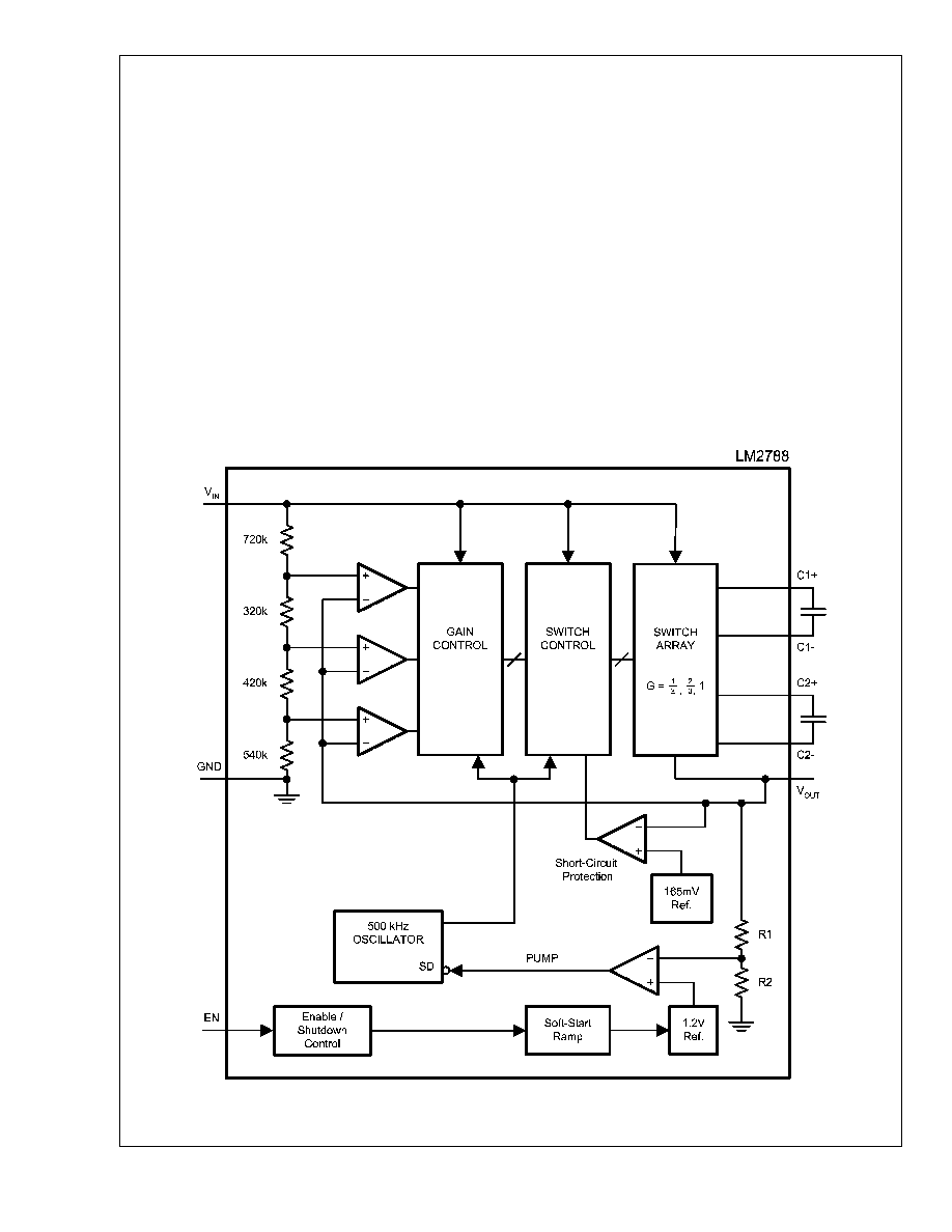
Block Diagram
20044403
LM2788
www.national.com
4
相關(guān)PDF資料 |
PDF描述 |
|---|---|
| LM2788MM-1.5/NOPB | SWITCHED CAPACITOR REGULATOR, 500 kHz SWITCHING FREQ-MAX, PDSO8 |
| LM2788MMX-1.5/NOPB | SWITCHED CAPACITOR REGULATOR, 500 kHz SWITCHING FREQ-MAX, PDSO8 |
| LM2794BL/NOPB | SWITCHED CAPACITOR REGULATOR, 675 kHz SWITCHING FREQ-MAX, PBGA14 |
| LM2797MM-1.8/NOPB | 0.12 A SWITCHED CAPACITOR REGULATOR, PDSO10 |
| LM2797MMX-1.8/NOPB | 0.12 A SWITCHED CAPACITOR REGULATOR, PDSO10 |
相關(guān)代理商/技術(shù)參數(shù) |
參數(shù)描述 |
|---|---|
| LM2788MMX-1.5 | 制造商:NSC 制造商全稱:National Semiconductor 功能描述:120mA High Efficiency Step-Down Switched Capacitor Voltage Converter |
| LM2788MMX-1.8 | 制造商:NSC 制造商全稱:National Semiconductor 功能描述:120mA High Efficiency Step-Down Switched Capacitor Voltage Converter |
| LM2788MMX-2.0 | 制造商:NSC 制造商全稱:National Semiconductor 功能描述:120mA High Efficiency Step-Down Switched Capacitor Voltage Converter |
| LM2791 | 制造商:NSC 制造商全稱:National Semiconductor 功能描述:Current Regulated Switched Capacitor LED Driver with Analog Brightness Control |
| LM2791B WAF | 制造商:Texas Instruments 功能描述: |
發(fā)布緊急采購(gòu),3分鐘左右您將得到回復(fù)。