- 您現(xiàn)在的位置:買賣IC網(wǎng) > PDF目錄44549 > LM2641-ADJMDC (NATIONAL SEMICONDUCTOR CORP) DUAL SWITCHING CONTROLLER, 345 kHz SWITCHING FREQ-MAX, UUC PDF資料下載
參數(shù)資料
| 型號(hào): | LM2641-ADJMDC |
| 廠商: | NATIONAL SEMICONDUCTOR CORP |
| 元件分類: | 穩(wěn)壓器 |
| 英文描述: | DUAL SWITCHING CONTROLLER, 345 kHz SWITCHING FREQ-MAX, UUC |
| 封裝: | DIE |
| 文件頁數(shù): | 20/22頁 |
| 文件大小: | 531K |
| 代理商: | LM2641-ADJMDC |
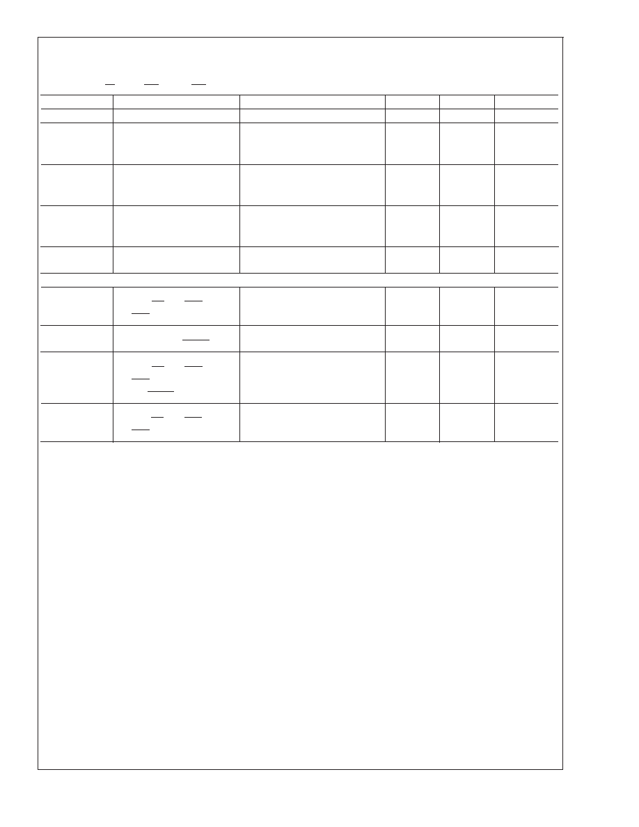
Electrical Characteristics (Continued)
Typicals and limits appearing in regular type apply for T
J = 25C. Limits appearing in boldface type apply over the entire junc-
tion temperature range for operation, 0 to +125C. Unless otherwise specified under the Parameter or Conditions columns, V
IN
= 10V, and V
Symbol
Parameter
Conditions
Typical
Limit
Units
V
BG
Bandgap Voltage
1.238
V
REF
Reference Voltage
0.01 mA
≤ I
REF ≤ 5 mA Source,
V
LIN ≤ 6V
2.5
V
2.45
V(min)
2.55
V(max)
V
LIN
Output Voltage of the Linear
Voltage Regulator
6V
≤ V
IN ≤ 30V,
0mA
≤ I
LIN ≤ 25 mA
5V
4.6
V(min)
5.4
V(max)
V
UVLO
Undervoltage Lockout
Threshold
4.0
V
3.6
V(min)
4.4
V(max)
LIN-to-V
OUT Switch-Over
Threshold
V
OUT taken at CSL1
4.8
V
Logic Inputs
V
IH
Minimum High Level Input
Voltage (SD, ON/OFF1,
ON/OFF2, and SYNC)
2.4
V(min)
V
IH
Minimum High Level Input
Voltage (2NDFB/FPWM)
2.6
V(min)
V
IL
Maximum Low Level Input
Voltage (SD, ON/OFF1,
ON/OFF2, SYNC, and
2NDFB/FPWM)
0.8
V(max)
Maximum Input Leakage
Current (SD, ON/OFF1,
ON/OFF2, and SYNC)
Logic Input Voltage 0 or 5V
±0.1
A
Note 1: Unless otherwise specified, all voltages are with respect to the voltage at the GND and PGND pins.
Note 2: Absolute Maximum Ratings are limits beyond which damage to the device may occur. Operating Ratings are conditions under which operation of the device
is guaranteed. Operating Ratings do not imply guaranteed performance limits. For guaranteed performance limits and associated test conditions, see the Electrical
Characteristics tables.
Note 3: The Absolute Maximum power dissipation depends on the ambient temperature. The 883 mW rating results from substituting 150C, 70C, and 90.6C/W
for TJmax,TA, and θJA respectively into the formula Pmax =(TJmax -TA)/θJA, where Pmax is the Absolute Maximum power dissipation, TJmax is the Absolute Maximum
junction temperature, TA is the ambient temperature, and θJA is the junction-to-ambient thermal resistance of the package. A θJA of 90.6C/W represents the
worst-case condition of no heat sinking of the 28-pin TSSOP. Heat sinking allows the safe dissipation of more power. The Absolute Maximum power dissipation must
be derated by 11.04 mW per C above 70C ambient. The LM2641 actively limits its junction temperature to about 150C.
Note 4: For detailed information on soldering plastic small-outline packages, refer to the Packaging Databook available from National Semiconductor Corporation.
Note 5: For testing purposes, ESD was applied using the human-body model, a 100 pF capacitor discharged through a 1.5 k
resistor.
Note 6: A typical is the center of characterization data taken with TA =TJ = 25C. Typicals are not guaranteed.
Note 7: All limits are guaranteed. All electrical characteristics having room-temperature limits are tested during production with TA = 25C. All hot and cold limits are
guaranteed by correlating the electrical characteristics to process and temperature variations and applying statistical process control.
Note 8: Both controllers are ON but not switching. Currents entering the IC at IN, CSL1, CSH1, CSL2, and CSH2 are measured. Those entering at CSL1 and CSH1
are multiplied by 0.50 to emulate the effect of a switching conversion from 10V down to 5V. Those entering at CSL2 and CSH2 are multiplied by 0.33 to emulate
the effect of a switching conversion from 10V down to 3.3V. After multiplication, all five currents are added. Because the voltage at the CSL1 input is greater than
the LIN-to-VOUT switchover threshold, most of the input supply current enters the IC via the CSL1 input.
Note 9: Both switching controllers are OFF. The 5V, 50 mA linear regulator (output at LIN) and the precision 2.5V reference (output at REF) remain ON.
Note 10: Both switching controllers and the 2.5V precision reference are OFF. The 5V, 50 mA linear regulator remains ON.
Note 11: The controllers remain OFF until the voltage of the 5V, 50 mA linear regulator (output at LIN) reaches this threshold.
Note 12: In applications where the output voltage can exceed the absolute maximum rating, a 100
resistor must be placed in series with the CSH and CSL inputs.
LM2641
www.national.com
7
相關(guān)PDF資料 |
PDF描述 |
|---|---|
| LM2645MTD/NOPB | SWITCHING CONTROLLER, 335 kHz SWITCHING FREQ-MAX, PDSO48 |
| LM2651MTCX-2.5/NOPB | 2.6 A SWITCHING REGULATOR, 345 kHz SWITCHING FREQ-MAX, PDSO16 |
| LM2651MTC-2.5/NOPB | 2.6 A SWITCHING REGULATOR, 345 kHz SWITCHING FREQ-MAX, PDSO16 |
| LM2651MTC-1.8/NOPB | 2.6 A SWITCHING REGULATOR, 345 kHz SWITCHING FREQ-MAX, PDSO16 |
| LM2670-5.0MDC | 5.4 A SWITCHING REGULATOR, 280 kHz SWITCHING FREQ-MAX, UUC |
相關(guān)代理商/技術(shù)參數(shù) |
參數(shù)描述 |
|---|---|
| LM2641MTC-ADJ | 功能描述:DC/DC 開關(guān)控制器 RoHS:否 制造商:Texas Instruments 輸入電壓:6 V to 100 V 開關(guān)頻率: 輸出電壓:1.215 V to 80 V 輸出電流:3.5 A 輸出端數(shù)量:1 最大工作溫度:+ 125 C 安裝風(fēng)格: 封裝 / 箱體:CPAK |
| LM2641MTC-ADJ/NOPB | 功能描述:DC/DC 開關(guān)控制器 RoHS:否 制造商:Texas Instruments 輸入電壓:6 V to 100 V 開關(guān)頻率: 輸出電壓:1.215 V to 80 V 輸出電流:3.5 A 輸出端數(shù)量:1 最大工作溫度:+ 125 C 安裝風(fēng)格: 封裝 / 箱體:CPAK |
| LM2641MTCX-ADJ | 功能描述:DC/DC 開關(guān)控制器 RoHS:否 制造商:Texas Instruments 輸入電壓:6 V to 100 V 開關(guān)頻率: 輸出電壓:1.215 V to 80 V 輸出電流:3.5 A 輸出端數(shù)量:1 最大工作溫度:+ 125 C 安裝風(fēng)格: 封裝 / 箱體:CPAK |
| LM2641MTCX-ADJ/NOPB | 功能描述:DC/DC 開關(guān)控制器 RoHS:否 制造商:Texas Instruments 輸入電壓:6 V to 100 V 開關(guān)頻率: 輸出電壓:1.215 V to 80 V 輸出電流:3.5 A 輸出端數(shù)量:1 最大工作溫度:+ 125 C 安裝風(fēng)格: 封裝 / 箱體:CPAK |
| LM2642 | 制造商:未知廠家 制造商全稱:未知廠家 功能描述: |
發(fā)布緊急采購,3分鐘左右您將得到回復(fù)。