- 您現(xiàn)在的位置:買(mǎi)賣IC網(wǎng) > PDF目錄44549 > LM2621MDC (NATIONAL SEMICONDUCTOR CORP) 2.85 A SWITCHING REGULATOR, 2000 kHz SWITCHING FREQ-MAX, UUC PDF資料下載
參數(shù)資料
| 型號(hào): | LM2621MDC |
| 廠商: | NATIONAL SEMICONDUCTOR CORP |
| 元件分類: | 穩(wěn)壓器 |
| 英文描述: | 2.85 A SWITCHING REGULATOR, 2000 kHz SWITCHING FREQ-MAX, UUC |
| 封裝: | DIE |
| 文件頁(yè)數(shù): | 7/13頁(yè) |
| 文件大小: | 306K |
| 代理商: | LM2621MDC |
第1頁(yè)第2頁(yè)第3頁(yè)第4頁(yè)第5頁(yè)第6頁(yè)當(dāng)前第7頁(yè)第8頁(yè)第9頁(yè)第10頁(yè)第11頁(yè)第12頁(yè)第13頁(yè)
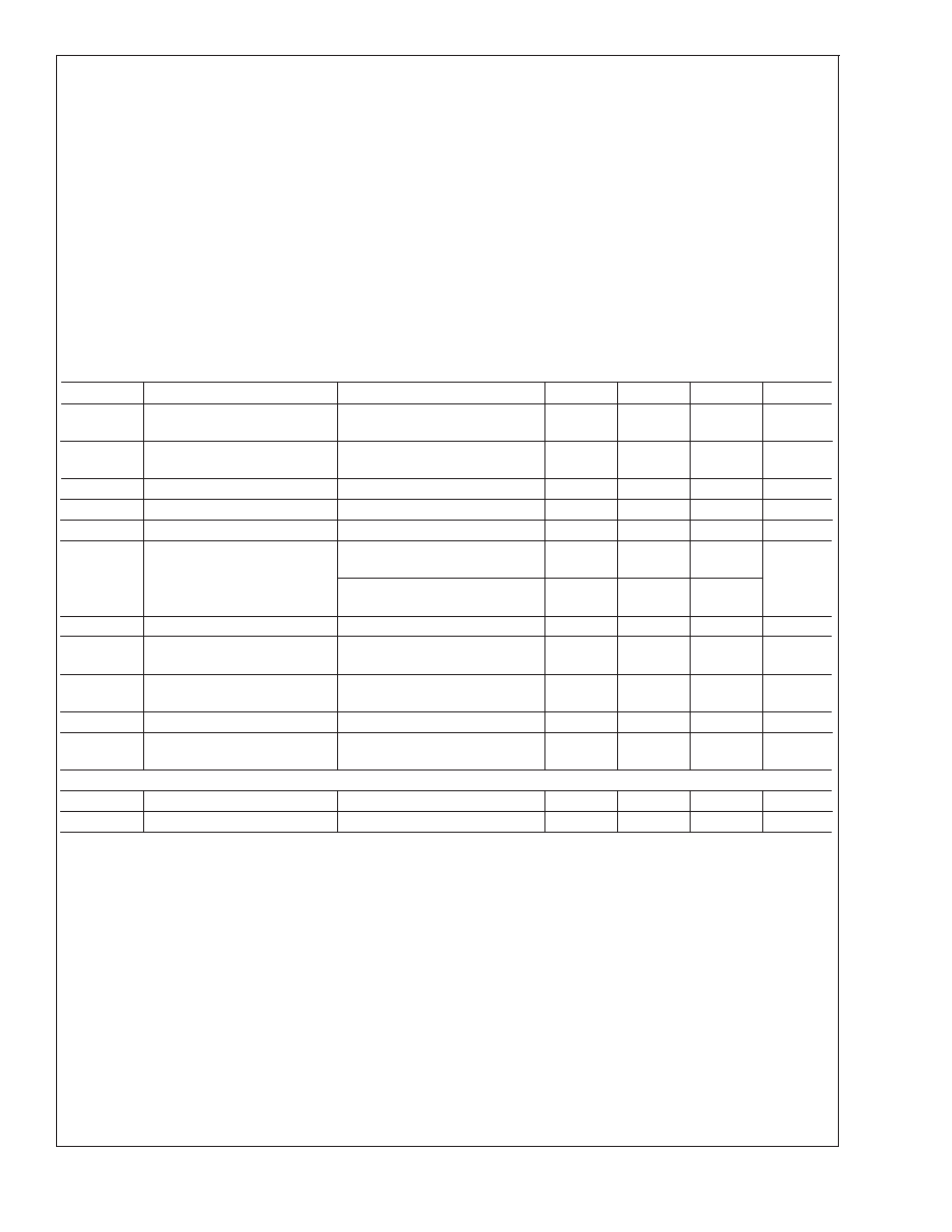
Absolute Maximum Ratings (Note 1)
If Military/Aerospace specified devices are required,
please contact the National Semiconductor Sales Office/
Distributors for availability and specifications.
SW Pin Voltage
0.5 V to 14.5V
BOOT, V
DD, EN and FB Pins
0.5V to 10V
FREQ Pin
100A
θ
JA (Note 2)
240C/W
T
Jmax (Note 2)
150C
Storage Temperature Range
65C to +150C
Lead Temp. (Soldering, 5 sec)
260C
Power Dissipation (T
A=25C)
(Note 2)
500mW
ESD Rating (Note 3)
2kV
Operating Conditions (Note 1)
V
DD Pin
2.5V to 5V
FB, EN Pins
0 to V
DD
BOOT Pin
0 to 10V
Ambient Temperature (T
A)
40C to +85C
Electrical Characteristics
Limits in standard typeface are for T
J = 25C, and limits in boldface type apply over the full operating temperature range of
40C to +85C. Unless otherwise specified: V
DD=VOUT= 3.3V.
Symbol
Parameter
Condition
Typ
Min
Max
Units
V
IN_ST
Minimum Start-Up Supply
Voltage (Note 4)
I
LOAD = 0mA
1.1
1.2
V
IN_OP
Minimum Operating Supply
Voltage (once started)
I
LOAD = 0mA
0.65
V
FB
FB Pin Voltage
1.24
1.2028
1.2772
V
OUT_MAX
Maximum Output Voltage
14
V
HYST
Hysteresis Voltage (Note 7)
30
45
mV
η
Efficiency
V
IN = 3.6V; VOUT = 5V; ILOAD
= 500mA
87
%
V
IN = 2.5V; VOUT = 3.3V; ILOAD
= 200mA
87
D
Switch Duty Cycle
70
60
80
%
I
DD
Operating Quiescent Current
(Note 6)
FB Pin > 1.3V; EN Pin at V
DD
80
110
A
I
SD
Shutdown Quiescent Current
(Note 7)
V
DD, BOOT and SW Pins at
5.0V; EN Pin <200mV
0.01
2.5
A
I
CL
Switch Peak Current Limit
2.85
A
R
DS_ON
MOSFET Switch On
Resistance
0.17
Enable Section
V
EN_LO
EN Pin Voltage Low (Note 8)
0.15V
DD
V
EN_HI
EN Pin Voltage High (Note 8)
0.7V
DD
V
Note 1: Absolute maximum ratings indicate limits beyond which damage to the device may occur. Electrical specifications do not apply when operating the device
outside of its rated operating conditions.
Note 2: The maximum power dissipation must be derated at elevated temperatures and is dictated by Tjmax (maximum junction temperature), θJA (junction to am-
bient thermal resistance), and TA (ambient temperature). The maximum allowable power dissipation at any temperature is Pdmax =(Tjmax -TA)/ θJA or the number
given in the Absolute Maximum Ratings, whichever is lower.
Note 3: The human body model is a 100 pF capacitor discharged through a 1.5 k
resistor into each pin. For Pin 8 (SW) the ESD rating is 1.5 kV.
Note 4: Output in regulation, VOUT =VOUT (NOMINAL) ± 5%
Note 5: This is the hysteresis value of the internal comparator used for the gated-oscillator control scheme.
Note 6: This is the current into the VDD pin.
Note 7: This is the total current into pins VDD, BOOT, SW and FREQ.
Note 8: When the EN pin is below VEN_LO, the regulator is shut down; when it is above VEN_HI, the regulator is operating.
LM2621
www.national.com
3
相關(guān)PDF資料 |
PDF描述 |
|---|---|
| LM2622-ADJMWC | 2.3 A SWITCHING REGULATOR, 1500 kHz SWITCHING FREQ-MAX, UUC |
| LM2630MTC-ADJ/NOPB | SWITCHING CONTROLLER, 345 kHz SWITCHING FREQ-MAX, PDSO20 |
| LM2630MTC-ADJX | SWITCHING CONTROLLER, 345 kHz SWITCHING FREQ-MAX, PDSO20 |
| LM2631MTCX-ADJ/NOPB | SWITCHING CONTROLLER, 400 kHz SWITCHING FREQ-MAX, PDSO20 |
| LM2636MWC | SWITCHING CONTROLLER, 2000 kHz SWITCHING FREQ-MAX, UUC |
相關(guān)代理商/技術(shù)參數(shù) |
參數(shù)描述 |
|---|---|
| LM2621MM | 功能描述:DC/DC 開(kāi)關(guān)控制器 RoHS:否 制造商:Texas Instruments 輸入電壓:6 V to 100 V 開(kāi)關(guān)頻率: 輸出電壓:1.215 V to 80 V 輸出電流:3.5 A 輸出端數(shù)量:1 最大工作溫度:+ 125 C 安裝風(fēng)格: 封裝 / 箱體:CPAK |
| LM2621MM | 制造商:Texas Instruments 功能描述:DC/DC UP CONVERTER ADJ SMD 2621 |
| LM2621MM/NOPB | 功能描述:DC/DC 開(kāi)關(guān)控制器 LOW INP VLTG,STEP-UP DC-DC RoHS:否 制造商:Texas Instruments 輸入電壓:6 V to 100 V 開(kāi)關(guān)頻率: 輸出電壓:1.215 V to 80 V 輸出電流:3.5 A 輸出端數(shù)量:1 最大工作溫度:+ 125 C 安裝風(fēng)格: 封裝 / 箱體:CPAK |
| LM2621MM/NOPB | 制造商:Texas Instruments 功能描述:DC/DC Converter (DC-DC) / Switching Regu |
| LM2621MMX | 功能描述:DC/DC 開(kāi)關(guān)控制器 RoHS:否 制造商:Texas Instruments 輸入電壓:6 V to 100 V 開(kāi)關(guān)頻率: 輸出電壓:1.215 V to 80 V 輸出電流:3.5 A 輸出端數(shù)量:1 最大工作溫度:+ 125 C 安裝風(fēng)格: 封裝 / 箱體:CPAK |
發(fā)布緊急采購(gòu),3分鐘左右您將得到回復(fù)。