- 您現(xiàn)在的位置:買賣IC網(wǎng) > PDF目錄44548 > LM2575TV-5.0 (MOTOROLA INC) 3.2 A SWITCHING REGULATOR, 63 kHz SWITCHING FREQ-MAX, PZFM5 PDF資料下載
參數(shù)資料
| 型號: | LM2575TV-5.0 |
| 廠商: | MOTOROLA INC |
| 元件分類: | 穩(wěn)壓器 |
| 英文描述: | 3.2 A SWITCHING REGULATOR, 63 kHz SWITCHING FREQ-MAX, PZFM5 |
| 封裝: | 314B-05 |
| 文件頁數(shù): | 23/28頁 |
| 文件大小: | 380K |
| 代理商: | LM2575TV-5.0 |
第1頁第2頁第3頁第4頁第5頁第6頁第7頁第8頁第9頁第10頁第11頁第12頁第13頁第14頁第15頁第16頁第17頁第18頁第19頁第20頁第21頁第22頁當前第23頁第24頁第25頁第26頁第27頁第28頁
LM2575
4
MOTOROLA ANALOG IC DEVICE DATA
DEVICE PARAMETERS
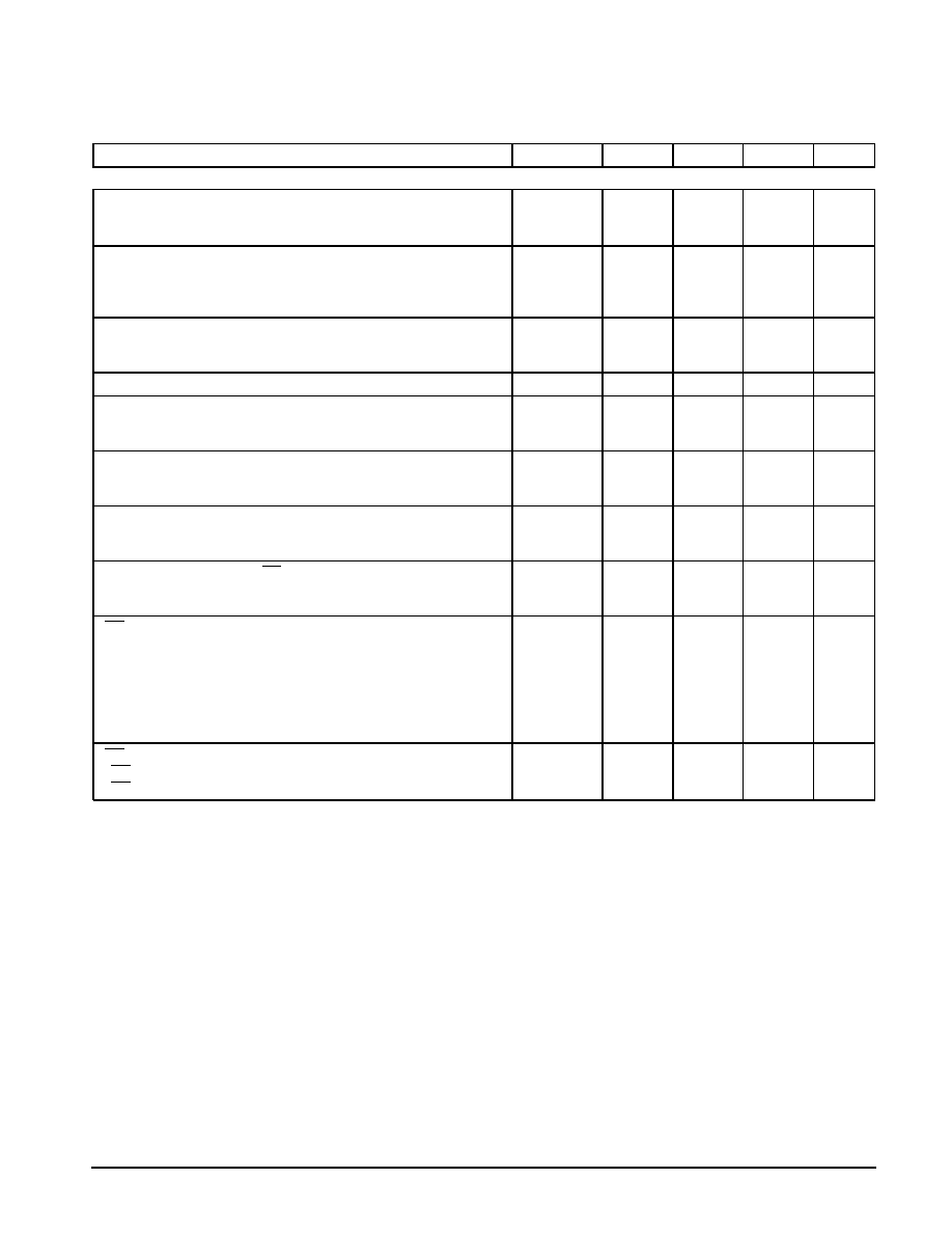
ELECTRICAL CHARACTERISTICS (Unless otherwise specified, Vin = 12 V for the 3.3 V, 5.0 V, and Adjustable version, Vin = 25 V for
the 12 V version, and Vin = 30 V for the 15 V version. ILoad = 200 mA. For typical values TJ = 25°C, for min/max values TJ is the operating
junction temperature range that applies [Note 2], unless otherwise noted.)
Characteristics
Symbol
Min
Typ
Max
Unit
ALL OUTPUT VOLTAGE VERSIONS
Feedback Bias Current (Vout = 5.0 V [Adjustable Version Only])
Ib
nA
TJ = 25°C
–
25
100
TJ = –40 to +125°C
–
200
Oscillator Frequency [Note 3]
fosc
kHz
TJ = 25°C
–
52
–
TJ = 0 to +125°C
47
–
58
TJ = –40 to +125°C
42
–
63
Saturation Voltage (Iout = 1.0 A [Note 4])
Vsat
V
TJ = 25°C
–
1.0
1.2
TJ = –40 to +125°C
–
1.3
Max Duty Cycle (“on”) [Note 5]
DC
94
98
–
%
Current Limit (Peak Current [Notes 4 and 3])
ICL
A
TJ = 25°C
1.7
2.3
3.0
TJ = –40 to +125°C
1.4
–
3.2
Output Leakage Current [Notes 6 and 7], TJ = 25°C
IL
mA
Output = 0 V
–
0.8
2.0
Output = –1.0 V
–
6.0
20
Quiescent Current [Note 6]
IQ
mA
TJ = 25°C
–
5.0
9.0
TJ = –40 to +125°C
–
11
Standby Quiescent Current (ON/OFF Pin = 5.0 V (“off”))
Istby
A
TJ = 25°C
–
80
200
TJ = –40 to +125°C
–
400
ON/OFF Pin Logic Input Level (Test Circuit Figure 14)
V
Vout = 0 V
VIH
TJ = 25°C
2.2
1.4
–
TJ = –40 to +125°C
2.4
–
Vout = Nominal Output Voltage
VIL
TJ = 25°C
–
1.2
1.0
TJ = –40 to +125°C
–
0.8
ON/OFF Pin Input Current (Test Circuit Figure 14)
A
ON/OFF Pin = 5.0 V (“off”), TJ = 25°C
IIH
–
15
30
ON/OFF Pin = 0 V (“on”), TJ = 25°C
IIL
–
0
5.0
NOTES: 3. The oscillator frequency reduces to approximately 18 kHz in the event of an output short or an overload which causes the regulated output voltage to
drop approximately 40% from the nominal output voltage. This self protection feature lowers the average dissipation of the IC by lowering the
minimum duty cycle from 5% down to approximately 2%.
4. Output (Pin 2) sourcing current. No diode, inductor or capacitor connected to output pin.
5. Feedback (Pin 4) removed from output and connected to 0 V.
6. Feedback (Pin 4) removed from output and connected to +12 V for the Adjustable, 3.3 V, and 5.0 V versions, and +25 V for the 12 V and 15 V
versions, to force the output transistor “off”.
7. Vin = 40 V.
相關(guān)PDF資料 |
PDF描述 |
|---|---|
| LM2575T-3.3 | 3.2 A SWITCHING REGULATOR, 52 kHz SWITCHING FREQ-MAX, PSFM5 |
| LM2575TV-ADJ | 3.2 A SWITCHING REGULATOR, 52 kHz SWITCHING FREQ-MAX, PZFM5 |
| LM2576S-ADJT | 7.5 A SWITCHING REGULATOR, 62 kHz SWITCHING FREQ-MAX, PSSO5 |
| LM2576S-ADJ | 7.5 A SWITCHING REGULATOR, 62 kHz SWITCHING FREQ-MAX, PSSO5 |
| LM2575S-ADJT | 3.2 A SWITCHING REGULATOR, 62 kHz SWITCHING FREQ-MAX, PSSO5 |
相關(guān)代理商/技術(shù)參數(shù) |
參數(shù)描述 |
|---|---|
| LM2575TV-5G | 功能描述:直流/直流開關(guān)調(diào)節(jié)器 5V 1A PWR SW REG RoHS:否 制造商:International Rectifier 最大輸入電壓:21 V 開關(guān)頻率:1.5 MHz 輸出電壓:0.5 V to 0.86 V 輸出電流:4 A 輸出端數(shù)量: 最大工作溫度: 安裝風格:SMD/SMT 封裝 / 箱體:PQFN 4 x 5 |
| LM2575TV-ADJ | 功能描述:直流/直流開關(guān)調(diào)節(jié)器 1A 1.23-37V ADJ Buck RoHS:否 制造商:International Rectifier 最大輸入電壓:21 V 開關(guān)頻率:1.5 MHz 輸出電壓:0.5 V to 0.86 V 輸出電流:4 A 輸出端數(shù)量: 最大工作溫度: 安裝風格:SMD/SMT 封裝 / 箱體:PQFN 4 x 5 |
| LM2575TV-ADJG | 功能描述:直流/直流開關(guān)調(diào)節(jié)器 1A 1.23-37V ADJ Buck PWM RoHS:否 制造商:International Rectifier 最大輸入電壓:21 V 開關(guān)頻率:1.5 MHz 輸出電壓:0.5 V to 0.86 V 輸出電流:4 A 輸出端數(shù)量: 最大工作溫度: 安裝風格:SMD/SMT 封裝 / 箱體:PQFN 4 x 5 |
| LM2575WT | 功能描述:直流/直流開關(guān)調(diào)節(jié)器 1A Step-Down SMPS Regulator (ROHS Compliant) RoHS:否 制造商:International Rectifier 最大輸入電壓:21 V 開關(guān)頻率:1.5 MHz 輸出電壓:0.5 V to 0.86 V 輸出電流:4 A 輸出端數(shù)量: 最大工作溫度: 安裝風格:SMD/SMT 封裝 / 箱體:PQFN 4 x 5 |
| LM2575WU | 功能描述:直流/直流開關(guān)調(diào)節(jié)器 1A Step-Down SMPS Regulator (ROHS Compliant) RoHS:否 制造商:International Rectifier 最大輸入電壓:21 V 開關(guān)頻率:1.5 MHz 輸出電壓:0.5 V to 0.86 V 輸出電流:4 A 輸出端數(shù)量: 最大工作溫度: 安裝風格:SMD/SMT 封裝 / 箱體:PQFN 4 x 5 |
發(fā)布緊急采購,3分鐘左右您將得到回復。