- 您現(xiàn)在的位置:買賣IC網(wǎng) > PDF目錄358840 > LM123KSTEEL-MIL THREE-TERMINAL POSITIVE FIXED VOLTAGE REGULATORS PDF資料下載
參數(shù)資料
| 型號(hào): | LM123KSTEEL-MIL |
| 元件分類: | 基準(zhǔn)電壓源/電流源 |
| 英文描述: | THREE-TERMINAL POSITIVE FIXED VOLTAGE REGULATORS |
| 中文描述: | 三端固定電壓調(diào)節(jié)器 |
| 文件頁(yè)數(shù): | 5/8頁(yè) |
| 文件大小: | 126K |
| 代理商: | LM123KSTEEL-MIL |
LM323, A
5
MOTOROLA ANALOG IC DEVICE DATA
I
V
D
V
D
V
C
V
V
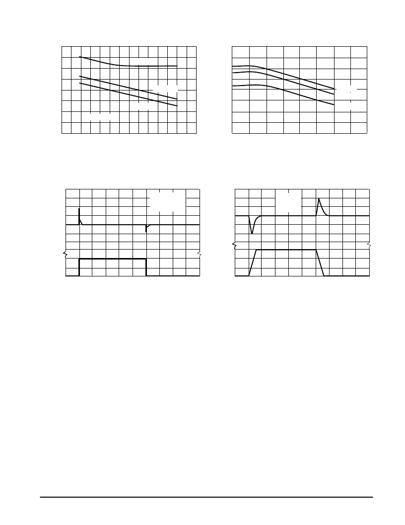
Figure 9. Dropout Voltage
Figure 10. Short Circuit Current
0
10
20
30
40
0.8
0.6
0.4
0.2
0
–0.2
–0.4
–0.6
1.0
0.5
0
t, TIME (
μ
s)
Iout = 150 mA
CO = 0
TJ = 25
°
C
1.0
C
0
10
20
30
40
t, TIME (
μ
s)
Vin = 10 V
CO = 0
TJ = 25
°
C
0.3
0.2
0.1
0
–0.1
–0.2
–0.3
1.5
0.5
0
Figure 11. Line Transient Response
Figure 12. Load Transient Response
2.5
2.0
1.5
1.0
0.5–90
–50
–10
30
70
110
150
190
TJ, JUNCTION TEMPERATURE (
°
C)
Iout = 3.0 A
Iout = 1.0 A
Iout = 0.5 A
Vout = 50 mV
8.0
6.0
4.0
2.0
05.0
10
15
20
25
S
I
Z
Vin, INPUT VOLTAGE (Vdc)
,
TJ = 0
°
C
TJ = 25
°
C
TJ = 125
°
C
APPLICATIONS INFORMATION
Design Considerations
The LM323,A series of fixed voltage regulators are
designed with Thermal Overload Protection that shuts down
the circuit when subjected to an excessive power overload
condition, Internal Short Circuit Protection that limits the
maximum current the circuit will pass, and Output Transistor
Safe–Area Compensation that reduces the output short
circuit current as the voltage across the pass transistor is
increased.
In many low current applications, compensation
capacitors are not required. However, it is recommended that
the regulator input be bypassed with a capacitor if the
regulator is connected to the power supply filter with long wire
lengths, or if the output load capacitance is large. An input
bypass capacitor should be selected to provide good
high–frequency characteristics to insure stable operation
under all load conditions. A 0.33
μ
F or larger tantalum, mylar,
or other capacitor having low internal impedance at high
frequencies should be chosen. The bypass capacitor should
be mounted with the shortest possible leads directly across
the regulator’s input terminals. Normally good construction
techniques should be used to minimize ground loops and
lead resistance drops since the regulator has no external
sense lead.
相關(guān)PDF資料 |
PDF描述 |
|---|---|
| LM323AT | 5.0 AMP POSITIVE VOLTAGE REGULATOR |
| LM323T | 5.0 AMP POSITIVE VOLTAGE REGULATOR |
| LM323AT | 5.0 AMP POSITIVE VOLTAGE REGULATOR |
| LM323T | 5.0 AMP POSITIVE VOLTAGE REGULATOR |
| LM323 | 5.0 AMP POSITIVE VOLTAGE REGULATOR |
相關(guān)代理商/技術(shù)參數(shù) |
參數(shù)描述 |
|---|---|
| LM123QML | 制造商:TI 制造商全稱:Texas Instruments 功能描述:LM123QML 3-Amp, 5-Volt Positive Regulator |
| LM123SM-05 | 制造商:SEME-LAB 制造商全稱:Seme LAB 功能描述:3 AMP POSITIVE VOLTAGE REGULATORS |
| LM123SM-12 | 制造商:SEME-LAB 制造商全稱:Seme LAB 功能描述:3 AMP POSITIVE VOLTAGE REGULATORS |
| LM123SM-15 | 制造商:SEME-LAB 制造商全稱:Seme LAB 功能描述:3 AMP POSITIVE VOLTAGE REGULATORS |
| LM123SMD-05 | 制造商:未知廠家 制造商全稱:未知廠家 功能描述:Voltage Regulator |
發(fā)布緊急采購(gòu),3分鐘左右您將得到回復(fù)。